Nowadays, digital electronic devices have a wide impact on our living. In our day to day activities, we use cell phones, PDA’s, and many more. These comprise comparators, Dividers, Adders, etc. The functionality and performance of this mainly depend on how efficiently these basic circuits operate. Full adder is beneficial in terms of the addition of multiple bits. Each circuit has its advantages and limitations based on the power supply and the propagation delay. Full Adder is the basic component of VLSI architecture. It is capable of performing arithmetic operations such as addition and subtraction. These digital circuits are obtained from the combination of logic gates. These systems designed with the gates are of two types either combinational or sequential. Full Adders are classified under the category of Combinational Logic Circuits. Because the output bits generated are dependent on the present input applied.
What is Full Adder?
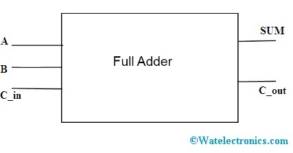
Definition: When the addition of two binary digits is performed, then the sum is generated. If it consists of two digits in the output then the MSB bit is referred to as carry. This is treated as the third bit in the process of addition. The ‘combinational circuit’ which is capable of performing addition on three input bits that is two inputs and the carry-in from the previous operation is known as Full Adder. The Block Diagram for this circuit is

Full Adder Block Diagram
In these circuits there are n input variables obtained from an external source are of binary type. The possible outputs combinations are 2^n. Each output generated can be expressed in terms of Boolean Function. The logic gates present in it acts based upon the signals applied. In digital systems, there are two levels of signals applied. Logic 1 is the higher level and Logic 0 which stands for a low level.
Full Adder Circuit Diagram, Truth Table and Equation
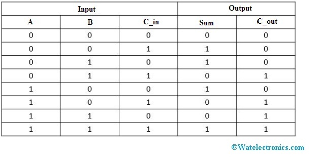
Three inputs are applied to this adder, then it produces (2^3) eight output combinations. The inputs are A, B, and Carry-in, and the outputs are Sum and Carry-out. The behavior of this circuit can be estimated from the truth table shown below.

Full Adder Truth Table
From the truth table, it can be concluded as
- When the three input bits applied are zero the outputs both sum and carry-out are zero.
- The sum output is 1 when only one of the input bit applied is 1 or when all the bits applied are 1.
- The carry-out can be 1 if two or three inputs applied are 1.
Based on the table the outputs can be realized in the form of the equation. These equations describe the outputs for any of the combinations.
s= A⊕B⊕Cin
Cout= AB+ACin+BCin
The equation for the output terminal of the sum is the exclusive operation performed on all the three inputs A, B, and Carry-in. Once the equations are obtained the logic diagram for the adder circuit is designed. Full adders are constructed using the basic logic gates. Even the combination of half adders can also lead to the formation of this adder.
Full Adder Circuit Using Basic Gates
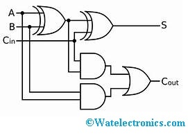
The two gates of XOR and AND followed by one OR gate can be utilized to construct the circuit of a full adder. The circuits comprise two half adder circuits. The purpose of the initial half adder is to generate the sum and carry but the carry-in is added at the next half adder circuit such that the final output is generated.
The circuit diagram of this adder with the basic gates is as follows:

Full Adder Circuit Diagram
The carry generated after the process in the half adder circuit is the OR function that obtains the final output for carry.
The implementation of this circuit becomes complex in comparison to the half-adder circuit as well as it increases the time required for the propagation of bits through the gates.
Applications
The applications of this circuit are
- The processors use this circuit to calculate the addresses of memory.
- In the Arithmetic and Logic Units, these circuits are present.
- The chips of processors like snapdragon, Intel and Exynos, etc… include this adder circuit
- Along with CPU’s the full adders are seen in Graphical Processing Units (GPUs).
- In the Timing and the Counting applications, these circuits are utilized.
- The domain of networks including digital signal processing full adder is the basic essential circuit.
Verilog Code
A Verilog code for the full adder of four bits which accepts the two inputs ‘a’ and ‘b’ each is of 4-bits length.
module fulladd (input [3:0] a, input [3:0] b, input c_in, output reg c_out, output reg [3:0] sum );
always @ (a or b or c_in) begin
{c-out, sum} = a+b+c_in;
end
endmodule
The code is written above consists of the keyword called ‘always’. This block in the code gets executed for a change in the input applied.
Please refer to this link to know more Logic Gates MCQs
FAQs
1). How many gates are there in Full Adder?
This circuit constructed using half adder circuitry it requires two XOR gates, two AND and one OR. If the same circuit is designed using universal gates such a NAND it consists of a total of 9 gates. Hence, the type of circuit design chosen decides the number of gates and its variants.
2). Why do we need Full Adder?
The addition of bits including carry-in is made possible by this full adder circuit. To perform the arithmetic operations on multiple bits we need this adder circuit. In the address calculation, Counting circuit to perform increment and decrement operations, in Calculators, etc… this circuit of the adder is used.
3). What are the Disadvantages of full adder?
The connection of individual gates for multiple bits processing results in the increase of the propagation delay. This overall affects time and power consumption. Due to the delay, the speed of the system gets affected. Even though this is a complete form of adder circuit these disadvantages needed to be fixed with the modifications in the circuit to achieve the efficient performance of the system.
4). What is a Hybrid full adder?
The combination of different logic forms to design a full adder is known as a hybrid full adder. For Example, a one-bit adder can be designed by using the CMOS technology with transmission and the pass transistor logic.
Please refer to this link to know more about XOR Gate MCQs, Binary Addition MCQs.
Please refer to this link to know more about VLSI Projects.
There is an advantage of a full adder circuit of one bit that by cascading it multiple bits addition can be performed. This kind of cascaded full adder is referred to as Ripple Carry Adder. Due to the cascading phenomenon is there any propagation delay generated in the circuit if yes then what would be the solution for it?