In electronic circuits, amplifiers are used to increase the strength or amplitude of the input signal without any phase change and frequency. Amplifier circuits are made up of either FET (Fied Effect Transistor) or normal bipolar junction transistor-based on their 3 terminals. The advantage of amplifier circuit using FET over BJTs is used as small-signal amplifiers because they produce high input impedance, high voltage gain, and low noise in the input signal. FET is a voltage-controlled device with three terminals -source, drain, and gate. Based on these terminals, FET is divided into 3 amplifier configuration that corresponding to 3 configurations of Bipolar transistors. They are common-source, common drain (source-follower), and common-gate amplifier circuits. The common – source amplifier circuit is most widely used than any other amplifier circuits because it can produce high input and output impedance, and also its performance is high. Here is a complete description of the common-source amplifier using FET.
What is a Common Source Amplifier
When the input signal is applied at the gate terminal and source terminal, then the output voltage is amplified and obtained across the resistor at the load in the drain terminal. This is called a common source amplifier. Here source acts as a common terminal between the input and output. It is also known as a voltage amplifier or a transconductance amplifier. It produces current gain and voltage gain according to the input impedance and output Impedance. To produce voltage gain along with high input impedances FET’s are used in these circuits.
Common Source Amplifier Circuit
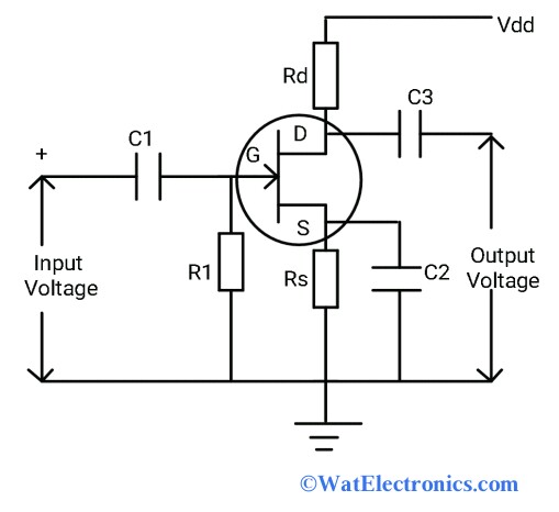
The circuit diagram of the common source amplifier with N-channel FET along with the coupling and biasing capability is shown below. This circuit will be similar to the common-emitter follower of Bipolar Junction transistor. If we use P-channel FET, the polarity of the input voltage will be reversed.

Common Source Amplifier Circuit
Design
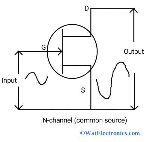
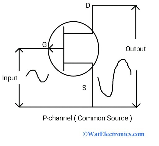
The design of a common source amplifier with FET is the same as the Class A amplifier using BJT (Bipolar Junction transistor). The design configuration of the common source amplifier using N-channel and P-channel FET is shown below.

N-channel (Common Source)

P-channel (Common Source)
The common source FET amplifier consists of 3 terminals. They are, source, gate, drain.
- Source: The majority of the source of carriers required for the device enters through this terminal. Through a source terminal, current enters the channel, which is denoted by IS
- Drain: The majority of the carriers in the channel leaves through this terminal. That is draining. Hence, conventional current enters the channel, which is denoted by ID.
- Gate: This terminal always controls the conductivity of the channel. Hence, the flow of current in the output is controlled with the help of a voltage level across the gate.
This amplifier can provide medium input Impedance, medium output impedance, medium current gain, medium voltage gain, reverse output with respect to input which means output signal will be in 180 degrees phase change. From these characteristics, we can conclude that this amplifier can give high-level performance over other amplifier circuits like a common drain (source follower) and common gate. Hence it is most widely used than other amplifier circuits.
Frequency Response
The frequency response of this amplifier is the most important factor. The circuit designs of low frequency and audio transistor circuits are different from RF applications. The capacitors and the type of FET used in the operation may affect the frequency response of the amplifier.
The frequency response of this amplifier is limited. This is the main drawback. The amplified output voltage can be applied to either a common-drain circuit ( voltage follower) or a common-gate circuit (current follower). To obtain better frequency response, common-drain and common-gate circuits are combined to form a cascade amplifier circuit.
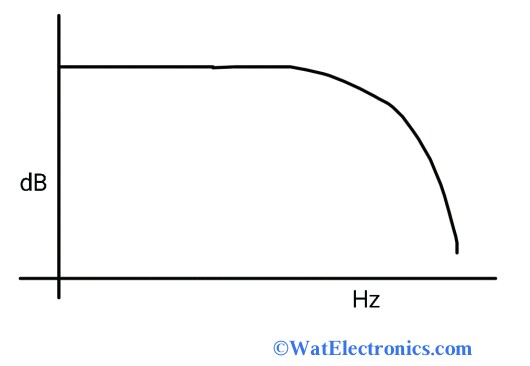
If the biasing arrangement is improper, then some form of distortion may appear in the amplified output signal. That is amplitude distortion, which can occur due to the effect of phase shift, clipping of signal, and also frequency distortion. The frequency response of this amplifier with active load is shown below

Frequency Response of Common Source Amplifier
Common Source Amplifier Working
This amplifier can work as either a transconductance amplifier or a voltage amplifier. If the amplifier is working as a transconductance amplifier, then the input signals are amplified and modulate the current flowing to the load. If the amplifier working as a voltage amplifier, then the input signal is amplified and modulates the current passing through the FET and changes the voltage across the load resistor according to the Ohm’s law.
The common source amplifier working can be explained from the above circuit diagram. Its working is similar to the working of a common-emitter follower of the BJT circuit.
When the input signal is applied at the gate terminal through the capacitor C1. The use of this capacitor is to check whether the gate terminal is affected by any DC voltage of the previous stage. The resistor R2 of around 1Mega ohms is between the gate and the ground holds the potential. The voltage is developed across the resistor R2 that can hold the source above the ground. The bypass capacitor C2 provides the additional gain for the AC signal. The amplified output voltage is obtained across the resistor R3 at the load at the drain terminal of the circuit. This amplified output voltage is coupled to the AC signal of the next stage by the capacitor C3 by blocking or eliminating the DC components. The amplified output signal of this amplifier is 180 degrees out of phase with respect to the input signal and produces high power gain.
The operation of the P-channel common source amplifier using FET is also similar to the N-channel common source amplifier FET except the voltage polarities will be reversed. In the reverse-biased state, there will be no current flowing between gate and source. Hence the gate current is zero. Then the gate voltage (DC) is given as,
Vg = Ig x Rg
The DC voltage at source is given by,
Vs = Id x Rs
Then the gate to source voltage is given by,
Vgs = Vg – Vs = 0- Id x Rs
Since Ig = 0
Vgs = – Id x Rs
Where
Id = drain current
Vgs = gate-source voltage
Vg = gate voltage
Rs = resistor at the source
Rg = resistor at Gate
Ig = gate current
The flow of DC components in the drain current can make the resistor Rs to provide self-biasing and feedback to the input from the output.
Applications
The applications of common source amplifier are as follows
- Used in amplification of sensor signals
- Used in low noise amplification of RF signals
- Used in communication systems like TV and FM receivers
- Used as voltage-controlled devices in op-amps
- Used as cascade amplifiers and RF amplifier circuits.
Please refer to this link to know more about Klystron Amplifier.
Please refer to this link to know more about Single Stage Transistor Amplifier & Negative Feedback MCQ’s.
Thus, this is all about the common source amplifier of single-stage N-channel FET – definition, circuit, design, working, frequency response, and applications. The purpose of this amplifier is, it can be used as either a transconductance amplifier or a voltage amplifier. It can provide high power gain, medium current, and voltage gains according to the input and output impedances. Here is a question to you, ” What are the V-I characteristics of common source amplifier?”