As the scope of digital technology and digital electronic circuits extends to many domains such as software, healthcare, automation, business and many, electronic representations of Boolean functions, numerous bands of logic gates are utilized to represent these digital signals. In the digital logic scenario, the output is completely a function of the current input. In a consequence of this process, logic gates that are used to represent digital circuits are categorized as sequential logic circuits and combinational logic circuits. As the implementation of the combinational logic circuits is in many computer circuits, let’s go ahead with the detailed discussion of how they operate, and many other conceptions related to this concept.
What is a Combinational Logic Circuit?
A combinational logic circuit as the name itself indicates that it is the combination of various kinds of logic gates. The combinational circuit goes with the characteristics of:
- At any instant of time, the output is based only on the levels of current input terminals and not on the past state inputs.
- These circuits do not need any kind of memory states or clock, so the past inputs show no influence on the current state of the circuit.
- A combinational circuit can intake ‘n’ number of inputs and delivers only one output.
Either the complicated or simple combinational logic, these can be represented through ‘NAND’, ‘NOT’ or ‘NOR gates’.

the basic combinational logic circuit
Representation of Combinational Logic Circuits
Here, we discuss the three approaches of representing combinational logic circuits
- Logic gates – These are the basic building blocks in the development of combinational logic circuits. NAND, NR, NOT, NOR, OR, AND are all logic gates.
- Boolean algebra – This representation stipulates the association that is between Boolean variables and is used to design digital circuitry through logic gates. Every digital system is basically designed with logic gates and so Boolean algebra is the one foremost approach to represent a combinational logic circuit.
- Truth table – This method computes the operational values of logical expressions for every combination of values taken by their logical variables. For every single-bit output in the logic block, a truth table is necessary to represent the logic. In general, all the output columns are represented in a single table.
For example, an expression that can be represented in the above three approaches as follows:
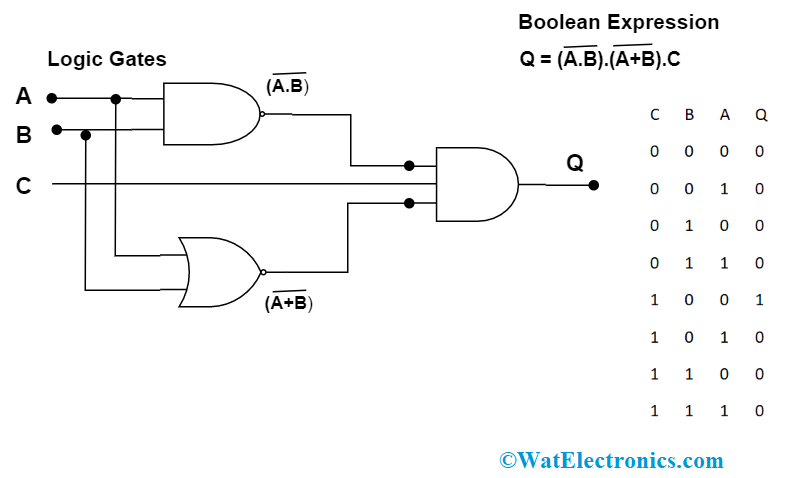
representation of combinational logic circuits
Classification of Combinational Logic Circuits
Combinational logic circuits are classified as below
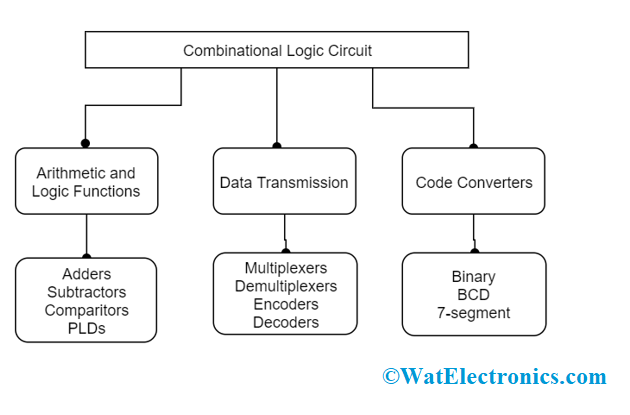
classification of combinational logic circuits
The foremost implementation of the combinational logic circuit is Multiplexer and de-multiplexer. In these, many numbers of inputs or outputs are on a single line and the logic gates are employed to decode corresponding output for the specified input.
Examples of Combinational Logic Circuits
The extensive implementation of combinational logic circuits today allowed us to discuss on a greater number of examples. Some of the real-life examples are as below:
Half Adder
It is the combinational logic derived by using two inputs and two outputs. The circuit design allowed us to add two one-bit binary numbers. So, the main purpose of using half adder is for addition. With the inputs as A and B, the circuit can be designed as follows
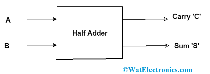
half adder block diagram
Truth Table
The output can be derived as below
|
Inputs |
Outputs | ||
| A |
B |
S |
C |
| L | L | L |
L |
|
L |
H | H |
L |
| H |
L |
H | L |
| H | H | L |
H |
Circuit Diagram
To gain the outputs Sum and Carry, the circuit is connected in the below format
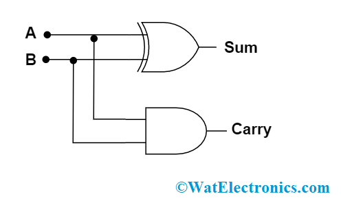
half adder circuit diagram
Full Adder
To surmount the disadvantage that is in half adder circuit, the full adder is designed. It holds the ability to add two binary numbers along with carrying input. So, it is the circuit with three inputs and two outputs.
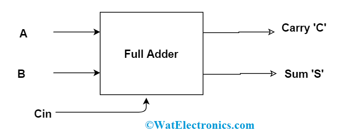
full adder block diagram
Truth Table
The output can be derived as below
|
Inputs |
Outputs | |||
| A | B | Cin | S |
C |
|
L |
L | L | L | L |
| L | L | H | H |
L |
|
L |
H | L | H | L |
| L | H | H | L |
H |
|
H |
L |
L | H | L |
| H | L | H | L |
H |
|
H |
H | L | L | H |
| H | H | H | H |
H |
Circuit Diagram
To gain the outputs Sum and Carry, the circuit is connected in the below format
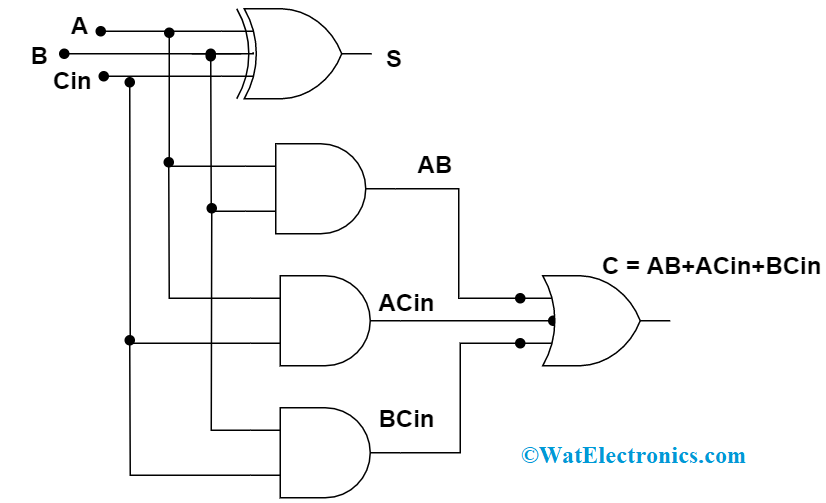
full adder circuit diagram
Note: As full adder holds the ability to add two one-bit binary numbers, in many cases we need to add n-bit numbers along with the carry. In those cases, an n-bit parallel adder holds the ability to add n-bit binary numbers. It is the combination of many full adders. So, the carry output of the previous adder is connected as an input to the next adder.
Half Subtractor
Accepting two binary numbers ‘A’ and ‘B’ as inputs, half subtractor derives the outputs borrow and difference. ‘Difference’ is the difference between two input numbers and while ‘Borrow’ is the one that carries borrow if any. In both the inputs, A is termed as Minuend and B is termed as Subtrahend.
Truth Table
The output can be derived as below
|
Inputs |
Outputs | ||
| A | B | Difference |
Borrow |
|
L |
L | L | L |
| L | H | H |
H |
|
H |
L | H | L |
| H | H | L |
L |
Circuit Diagram
To gain the outputs Difference and Borrow, the circuit is connected in the below format
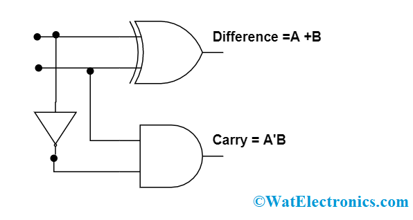
half subtractor circuit diagram
Full Subtractor
To take away the disadvantage of half-subtractor, a full subtractor is designed. The circuit is designed with three inputs that deliver two outputs one is Difference and Borrow. Where ‘Difference’ is the difference of two inputs and ‘Borrow’ is the carried borrow.
Truth Table
The delivered output from full subtractor is as below
|
Inputs |
Outputs | |||
| A | B | Cin | A-B-C |
Borrow |
|
L |
L |
L | L | L |
| L | L | H | H |
H |
|
L |
H |
L |
H |
H |
| L | H | H | L |
H |
|
H |
L | L | H | L |
| H | L | H | L |
L |
|
H |
H | L | L | L |
| H | H | H | H |
H |
Circuit Diagram
To gain the outputs Difference and Borrow, the circuit is connected in the below format
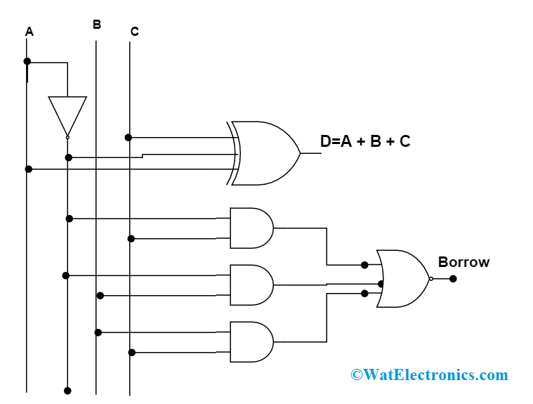
full subtractor circuit diagram
Note: Subtraction operation can be performed either by 1’s or 2’s complement of the number that has to be subtracted. For instance, we can carry out A-B either by the addition of 1’s or 2’s complement of B to the A input. So, here we make use of binary adder to carry out the subtraction process.
In detail, the process can be explained as:
• The subtracted number has to be passed through an inverter to get its complement.
• Then the 4-bit adder adds A and the complement of B and delivers subtraction results.
• When A>B and C is 0 and the result of A-B in binary format, then C =1 and the output is in 2’s complement form.
The below circuit diagram clearly explains the flow of the n-bit parallel subtractor.
Multiplexer
A multiplexer is the foremost application of a combinational logic circuit. The circuit has ‘n’ inputs, ‘m’ selection inputs with 2m = n and one output. This is the digital circuitry that chooses one data input and directs it to output. The selection of the inputs is carried out by selection inputs. Based on the applied digital code, one of the inputs is selected and addressed to the output. Cascading operation is performed by ‘E’ input which is the active low terminal input. The block diagram of the multiplexer is as follows
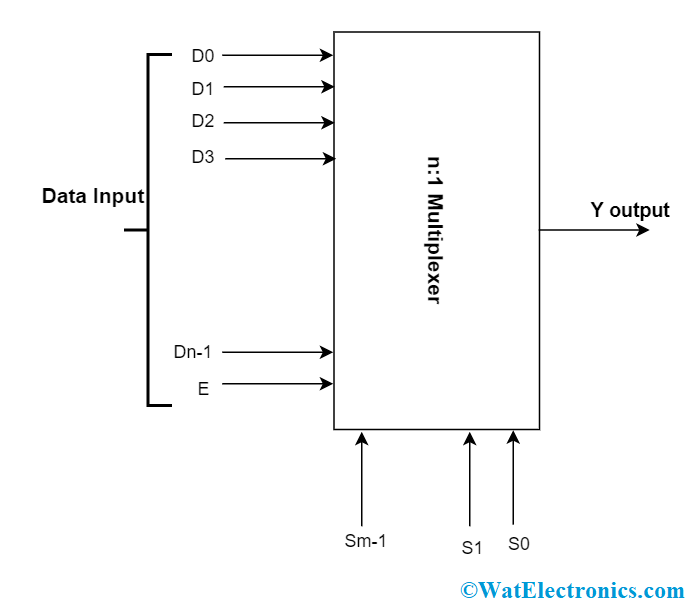
multiplexer
Multiplexers are used in many of the applications as because they are in available as
- 2:1 Mux
- 4:1 Mux
- 16:1 Mux
- 32:1 Mux
Let’s be clear with 2:1 Mux
Block Diagram – This is the basic block diagram of how a 2:1 mux operates
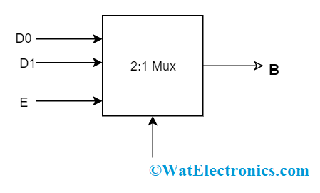
2-1 mux in the combinational logic circuit
Truth Table
The output can be derived as below
|
Enable |
Select |
Output |
|
E |
S | Y |
| H | × |
L |
|
H |
0 | D0 |
| H | H |
D1 |
Demultiplexer
A de-mux performs the operations reverse to that of a multiplexer. It has only one input and delivers multiple outputs. The circuit is designed with one input, ‘m’ select inputs and ‘n’ outputs. At a single instance, only one output is chosen through selection inputs and it is directed to the output. Demultiplexers are used in many of the applications as because they are in available as
- 1: 2 demux
- 1:4 demux
- 1:16 demux
- 1:32 demux
Let’s be clear with 1:2 demux
Block Diagram – This is the basic block diagram of how a 1:2 demux operates
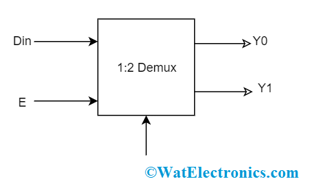
1-2 demux in the combinational logic circuit
Truth Table
The output can be derived as below.
|
Enable |
Select | Output | |
|
E |
S | Y0 |
Y1 |
| L | × | L |
L |
|
H |
L | L | Din |
| H | H | Din |
L |
Decoders, encoders, priority encoders are all examples of the combinational logic circuits.
Please refer to this link to know more about Combinational Logic Circuits MCQs
Applications of Combinational Logic Circuit
Combinational logic circuits are the basic building blocks of digital systems. They have an extensive variety of applications. They are used in
- Digital measuring techniques
- Digital processing
- Industrial processing
- Computers
- Calculators
- Digital Communication
Combinational logic circuits as arithmetic and logic circuits have applications as
- Comparators
- Programmable logic devices
- Adders & Subtractors
Combinational logic circuits as data transmission circuits have applications as
- Parallel to serial convertors
- Data routing
- Serial to parallel converters
- Bit Compression
- ADC and DAC
- Encoders & Decoders
Combinational logic circuits as code converter circuits have applications as
- Binary to gray code conversion
- Gray to Binary conversion
- BCD to Excess-3
- Excess-3 to BCD
- Seven segment code
Combinational Logic Circuit Design Procedure
The below steps clearly explains the design procedure of how a combinational logic system is developed
1. Identifying the required number of input and output variables
2. Symbolizing all the identified input and output variables
3. Express the relationship between these variables
4. With the relationship, construct the truth table
5. Derive the Boolean expression for all the outputs
6. Minimize the Boolean expression to reduce the complication
7. Design the logic diagram with the help of Boolean expressions
To minimize Boolean expressions, various approaches are followed. K-map and Quinne-McCluskey are the most followed techniques. The above-stated procedure is a streamlined and effective technique. Through this, the design of circuits seems to be completely reliable.
Is Multiplexer a Combinational Circuit?
Yes, Multiplexer is a combinational logic circuit that derives multiple outputs from the single input and it is designed through the combination of logic gates.
Is Flip Flop a Combinational Circuit?
No, Flip flop is an example of a sequential circuit that generates an output based on the sampled inputs and changes the output at certain intervals of time but not periodically.
The need for Combinational Circuits
Well, these days the scope of digital electronics gained utmost prominence and of the numerous elements, the one that received extensive prominence is combinational logic circuits. These circuits are the basic building blocks of digital systems. We need the implementation of these circuits to gain improved performance and they are employed in the operations that work with less power. Moreover, these are time-independent, and less implementation cost circuits and in processing the activities this feature helps the most.
Please refer to this link to know more Logic Gates MCQs
FAQs
1. How Boolean Algebra is used for?
It is the technique used to simplify and analyze digital logic. As it functions using the bits 0 and 1, it is also termed as Binary Algebra
2. What is the use of K-map?
Eliminating the complication involved in Boolean algebra theorems, manipulations and equations, k-map is the pictorial representation of reducing Boolean expressions.
3. State different types of multiplexers?
There are digital and analog multiplexers. Again, these are classified as Time Division Multiplexing (TDM), Frequency Division Multiplexing (FDM), and Wavelength Division Multiplexing (WDM).
4. What do you mean by multiplexing?
It is the process of transmitting multiple data streams through a communication link and then the receiver recovers individual signals.
5. What are Boolean operators?
There exist six boolean operators. They are AND, conditional AND, OR, conditional OR, exclusive OR, and NOT. Every argument that is passed to a logical operator has to be a boolean data type, and the output is always a boolean data type.
Please refer to this link to know more about Full Subtractor MCQs.
Get the foremost advantages of combinational logic circuits. Every electronic industry is based on these circuits and gaining the utmost prominence. So, know more about all other concepts and what are the other techniques and approaches in combinational logic circuits?