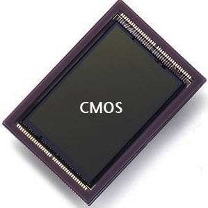
CMOS Fabrication
In early 1960’s the semiconductor manufacturing process was initiated from Texas and in 1963 CMOS or complementary metal oxide semiconductor was patented by Frank Wanlass. Integrated circuits are manufactured by utilizing the semiconductor device fabrication process. These ICs are major components of every electrical and electronic devices which we use in our daily life. Many complex and simple electronic circuits are being designed on a wafer made of semiconductor compounds and mostly silicon by using different fabrication steps.
The complementary of the Commodore Semiconductor Group (CSG) or Metal Oxide Semiconductor (MOS) is called as CMOS technology. This technology is used in developing the microprocessors, microcontrollers, digital logic circuits and many other integrated circuits. It facilitates low- power dissipation and high-packing density with very less noise margin. It is mostly used to build digital circuitry.
20 Steps of CMOS Fabrication Process
The CMOS can be fabricated using different processes such as:
- N-well process for CMOS fabrication
- P-well process
- Twin tub-CMOS-fabrication process
The fabrication of CMOS can be done by following the below shown twenty steps, by which CMOS can be obtained by integrating both the NMOS and PMOS transistors on the same chip substrate. For integrating these NMOS and PMOS devices on the same chip, special regions called as wells or tubs are required in which semiconductor type and substrate type are opposite to each other.
A P-well has to be created on a N-substrate or N-well has to be created on a P-substrate. In this article, the fabrication of CMOS is described using the P-substrate, in which the NMOS transistor is fabricated on a P-type substrate and the PMOS transistor is fabricated in N-well.
The fabrication process involves twenty steps, which are as follows:
Step1: Substrate
Primarily, start the process with a P-substrate.

Step2: Oxidation
The oxidation process is done by using high-purity oxygen and hydrogen, which are exposed in an oxidation furnace approximately at 1000 degree centigrade.

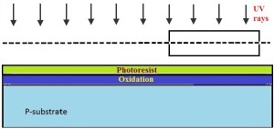
Step3: Photoresist
A light-sensitive polymer that softens whenever exposed to light is called as Photoresist layer. It is formed.

Step4: Masking
The photoresist is exposed to UV rays through the N-well mask
Step5: Photoresist removal
A part of the photoresist layer is removed by treating the wafer with the basic or acidic solution.
Step6: Removal of SiO2 using acid etching
The SiO2 oxidation layer is removed through the open area made by the removal of photoresist using hydrofluoric acid.

Step7: Removal of photoresist
The entire photoresist layer is stripped off, as shown in the below figure.

Step8: Formation of the N-well
By using ion implantation or diffusion process N-well is formed.

Step9: Removal of SiO2
Using the hydrofluoric acid, the remaining SiO2 is removed.
![]()
Step10: Deposition of polysilicon
Chemical Vapor Deposition (CVD) process is used to deposit a very thin layer of gate oxide.

Step11: Removing the layer barring a small area for the Gates
Except the two small regions required for forming the Gates of NMOS and PMOS, the remaining layer is stripped off.

Step12: Oxidation process
Next, an oxidation layer is formed on this layer with two small regions for the formation of the gate terminals of NMOS and PMOS.

Step13: Masking and N-diffusion
By using the masking process small gaps are made for the purpose of N-diffusion.

The n-type (n+) dopants are diffused or ion implanted, and the three n+ are formed for the formation of the terminals of NMOS.

Step14: Oxide stripping
The remaining oxidation layer is stripped off.img class=”aligncenter size-medium wp-image-1062″ src=”https://www.watelectronics.com/wp-content/uploads/14-300×64.jpg” alt=”” width=”300″ height=”64″ />
Step15: P-diffusion
Similar to the above N-diffusion process, the P-diffusion regions are diffused to form the terminals of the PMOS.

Step16: Thick field oxide
A thick-field oxide is formed in all regions except the terminals of the PMOS and NMOS.

Step17: Metallization
Aluminum is sputtered on the whole wafer.

Step18: Removal of excess metal
The excess metal is removed from the wafer layer.
 Step19: Terminals
The terminals of the PMOS and NMOS are made from respective gaps.

Step20: Assigning the names of the terminals of the NMOS and PMOS
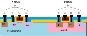
Fabircation of CMOS using P-well process
Among all the fabrication processes of the CMOS, N-well process is mostly used for the fabrication of the CMOS. P-well process is almost similar to the N-well. But the only difference in p-well process is that it consists of a main N-substrate and, thus, P-wells itself acts as substrate for the N-devices.
Twin tub-CMOS Fabrication Process
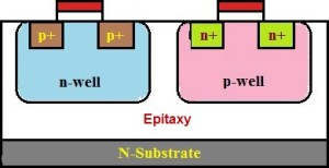
In this process, separate optimization of the n-type and p-type transistors will be provided. The independent optimization of Vt, body effect and gain of the P-devices, N-devices can be made possible with this process.
Different steps of the fabrication of the CMOS using the twintub process are as follows:
- Lightly doped n+ or p+ substrate is taken and, to protect the latch up, epitaxial layer is used.
- The high-purity controlled thickness of the layers of silicon are grown with exact dopant concentrations.
- The dopant and its concentration in Silicon are used to determine electrical properties.
- Formation of the tub
- Thin oxide construction
- Implantation of the source and drain
- Cuts for making contacts
- Metallization
By using the above steps we can fabricate CMOS using twintub process method.
CMOS Logic Gates
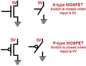
- The P-type and N-type transistors are called as fundamental building blocks of CMOS circuits.
- If the input voltage is low, then P-type MOSFET acts as closed switch and, if the input voltage is high, then the P-type MOSFET acts as open switch.
- If the input voltage is high, then the N-type MOSFET acts as a closed switch and, if input the voltage is low, then the N-type MOSFET acts as an open switch.
- Combining the P-type and N-type MOSFETs without any conduction path between the supply voltage and the ground is the basic idea behind developing the CMOS technology.
- With this combination, very little energy is consumed by the CMOS circuits.
CMOS Inverter
The below CMOS inverter circuit is the simplest CMOS logic gate which can be used as a light switch. If the input voltage is low (0V), then the transistor (P-type) T1 conducts (switch closed) while the transistor T2 doesn’t conduct (switch open). Hence, the output of the circuit will be equal to the supply voltage (5V).
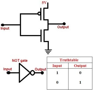
Similarly, if the input voltage is high (5V), then the transistor (N-type) T2 conducts (switch close) while the transistor T1 doesn’t conduct (switch open). Hence, the output of the circuit will be low (0V).
The above truth table shows the function of the CMOS inverter circuit and, from the table, we can observe that the output of the circuit is the inverse of the input.
Everytime whether the input is low or high, one of the two transistors conducts such that no current flows from the supply to ground.
Please refer to this link for CMOS MCQs.
For detailed information regarding the fabrication process of CMOS, which includes P-type and twintub processes and also advanced-fabrication process such as combination of Bipolar and CMOS ( BiCMOS fabrication), please post your ideas and queries by commenting below.
Please refer to this link to know more about CMOS and NMOS Technology & Operation of IGBT Circuit.