A tunnel diode was discovered by Leo Esaki in the year 1958. He noticed that if a semiconductor diode is doped heavily through impurities, then it will generate negative resistance that means the flow of current across the diode will decreases once the voltage enhances. Leo Esaki got the Nobel Prize in the physics subject for inventing the effect of electron tunneling that is used in these types of diodes in the year 1973. These diodes are one of the most important solid-state electronic components. As the name suggests, this diode is named after Leo Esaki for his tunneling effect work. This article discusses an overview of the tunneling effect and its working.
What is Tunnel Diode?
A semiconductor diode like a tunnel diode is also called an Esaki diode that has negative resistance because of the tunneling or quantum mechanical effect. This diode includes a heavily doped PN junction with 10 nm wide. In a semiconductor material, tunneling is the incident of conduction where the charge carrier hits the barrier rather than mounting through it.

Tunnel Diode
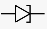
This kind of diode is used as a switching device with extreme speed in computers and also in amplifiers & high-frequency oscillators. The symbol of a tunnel diode is shown below where the p-type semiconductor works like an anode and the n-type semiconductor works like a cathode.

Tunnel Diode Symbol
Generally, an electrode-like anode is +vely charged that attracts electrons whereas a cathode is a negatively charged electrode that generates electrons. Alternatively, a p-type semiconductor attracts electrons which are generated from the n-type to the p-type is called the anode.
The operation of this diode mainly depends on the principle of quantum mechanics is called Tunneling. In electronics, tunneling is nothing but a direct electrons flow across the depletion region from one band to another like n-side conduction to the p-side valence.
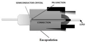
Tunnel Diode Construction
The materials used to make tunnel diode are germanium, gallium antimonide, silicon & gallium arsenide. This diode is designed with the two terminals like anode & cathode. Here, the semiconductor material like p-type works like an anode whereas the n-type works like a cathode.

Tunnel Diode Construction
In germanium material, the ratio of the peak value for the forward current toward the valley current value is highest & low for silicon. Therefore, silicon material is not utilized for constructing this diode. The diode doping density can be higher 1000 times as compared to the normal diode.
Working Principle
The working principle of tunnel diode is the same as a PN junction diode, except high doping density alters its conductivity equal to a huge extent. In a PN Junction diode, the concentration of doping is 1 atom within 108 atoms. However, in Tunnel Diode, the concentration of doping is 1 atom within 103 atoms. Because of the high impurity concentration of ions, the depletion layer width can be decreased & it turns into approximately 10-5mm.
Tunnel Diode Working
Once no voltage is applied or unbiased this diode, then the n-type semiconductor material’s conduction band partly covers through the p-type material’s valence band. So this occurs due to heavy doping. The holes and electrons energy levels within the P-type & N-type remain the same correspondingly.
Once the temperature increases, electrons burrow from the n-region of the conduction band to the p-region of the valence band. In the same way, the holes burrow from the p-regions valance band to the n-region conduction band. So in this condition, the diode will be unbiased which means there is no flow of current through the diode.
Once the small voltage is applied to this diode, then zero electrons flow across the depletion region & zero current supplies throughout the diode. In the n-region, the few electrons from the conduction band are burrow into the valence band in the p-region due to the burrowing of electrons, so little forward current will supply throughout the depletion region.
Once the high voltage is applied to the tunnel diode, then charge carriers like holes & electrons will be generated. When the applied voltage increases then both the bands will overlap and the energy levels at both bands in two regions will be equal. Therefore, the highest current flows through the tunnel.
Once the applied voltage is again highly increased then both the bands of the diode are misaligned slightly. However, both the bands in the two regions still overlap. The little current supplies throughout the diode then the tunnel current will start reducing.
If the conductor’s voltage is increasing heavily, the tunnel current will reduce to zero. In this state, both the bands will not overlap with each other, so this diode works like a normal PN-junction diode. As compared to built-in voltage, the voltage magnitude is higher than the forward current that will supply throughout the tunnel diode.
Circuit Diagram of Tunnel Diode
The circuit diagram of the tunnel diode is shown below. In the following diagram, the resistance of the connecting terminals of this diode & semiconductor material can be represented through ‘Rs’ that is equivalent to the 5 ohms. The inductance of the connecting terminals ‘Ls’ is almost equivalent to the 0.5nH. The junction diffusion capacitance ‘Cd’ & their magnitude ranges from 5-100pF.

Circuit Diagram
Main Terms used in Tunnel Diode
The related key terms used in tunnel diode are tunneling current, negative resistance characteristics & valley current.
The tunneling current is the flow of current throughout the device because of the electrons punching across the PN junction. The width of thin depletion permits some free electrons to burrow the junction instead of flying over it. The diffusion of electrons will produce a current called a Tunneling current.
The specific property like negative resistance characteristics is the particular capability of this diode where current signifies drop even once the voltage applied to it increases. Once tunneling attains its least value when the forward potential increases then, the least tunneling current value can be the device’s valley point.
Tunnel Diode VI Characteristics
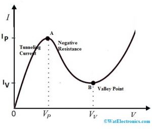
The VI characteristic of the tunnel diode is shown below. In this diode, heavy doping conduction can be occurred because of the forward biasing. The voltage applied to this diode is ‘Vp’ and the highest current reached by this diode is ‘Ip’. Once the high voltage is applied to this diode, then the value of current will be decreased.

VI Characteristics
The flow of current will decrease until it gets the least value, so the small current value is ‘Iv’.
From the following characteristic graph, we can notice that the flow of current will be reduced once voltage reduces. So, this is the region of negative resistance for this diode. The diode generates power in place of absorbing it.
Tunnel Diode Oscillator
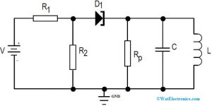
One of the applications of tunnel diode is the tunnel diode oscillator. If the tank circuit that includes an inductance (L) capacitance (C) & internal resistance (RP) is connected across the diode whose -ve resistance like –Rn & the net resistance like Req signifies RP & –Rn in parallel that can be given by
Req = -RnRp/Rp-Rn
If ‘Rp’ is higher than ‘Rn’, then ‘Req’ will be negative & oscillations can increase. After that, the amplitude of oscillation grows until it occupies a range of voltage that is higher than the amount of the negative resistance area of the characteristics.

Tunnel Diode Oscillator
Once the operating point goes into the positive resistance region, the amplitude of oscillation can be restricted. To get the utmost output, the inactive point should be precisely placed at the middle of the negative resistance area. So the oscillation frequency can be given by the following equation
F= 1/2π√LC
A tunnel diode includes a negative resistance region characteristic among the voltages 0.1 & 0.3V. It can be used as an oscillator at 100GHz frequencies. When the tunnel diode oscillator performs extremely well at extremely high frequencies, it cannot be utilized capably at fewer frequencies. This is the main disadvantage for the diode oscillator and it is also called a negative resistance oscillator.
Please refer to this link for Tunnel Diode MCQs.
Please refer to this link for Choosing resistor values for diodes.
Advantages
The advantages of tunnel diode include the following.
- The switching speed of this diode is high
- Long life
- This diode handles with high frequencies.
- Fabrication is simple
- Less noise & cost
- Power dissipation is low
- Operation is high speed
- Environmental protection
- The flow of current because of the majority charge carriers in this diode can respond very quickly to voltage changes. So, this property is extremely useful for high-speed applications.
- Huge current supplies at small reverse voltage value because of significant overlap in between two bands like valence & conduction. This is a very helpful property like a frequency converter.
- It generates a negative resistance feature that is used in oscillators & reflection amplifiers
Disadvantages
The disadvantages of tunnel diode include the following.
- These diodes are low-power devices.
- These are a bit expensive
- It delivers less o/p voltage swing.
- The ranges of power output are limited to simply a few milliwatts as the applied DC potential should be low as compared to the diode’s bandgap potential.
- There is no isolation among input &output as it is a 2-terminal device.
Applications
The applications of tunnel diode include the following.
- Tunnel diode is used in different oscillators like relaxation, microwave, etc.
- It is used as a switching device with very high speed.
- It is used like a logic memory storage device.
- It is used as a microwave oscillator with high frequency
- This diode is used as an oscillator, amplifier & switch
- It is used as a high-frequency component.
- It works as a storage device to store logic memory.
- It is used in FM receivers & oscillator circuits because it is a low-current device
know more about Varactor Diode MCQs.
Please refer to this link to know more about Isolation Amplifier.
Thus, this is all about an overview of the tunnel diode, construction, working, advantages, disadvantages & its applications. These diodes are used like an oscillator, amplifier, switch, etc. This diode can be used as a high-frequency component due to its quick response, however, it is not chosen because of the accessibility of better devices. Here is a question for you, what are the different types of diodes available in the market?