The transistor is one of the significant semiconductor components used in almost every electronic device to regulate or control electronic signal flow. The transistor is a kind of semiconductor device, used for conducting & insulating electric current (or) voltage. Transistors are available in two types; PNP and NPN. Generally, a transistor includes three terminals or layers that are made with semiconductor material to carry a current. Transistors are utilized in a broad range of electronic equipment or devices. Some common transistor applications are cell phones, computers, automotive, space, military, etc. There are different types of PNP and NPN transistors manufactured by different manufacturing companies. This article discusses an overview of one of the NPN transistors namely; the TIP41C transistor, pin configuration, specifications, circuit working, and its applications.
What is a TIP41C Transistor?
Tip41C is an NPN power transistor used for mainly switching & amplification purposes. This transistor belongs to the NPN category & comes with around 65 watts of high power, which is the released amount of energy while the transistor working. This NPN transistor comes in the TO-220 package which has temperature resistance capacity. This is a medium-power high-current NPN transistor that is used in power electronic circuits.
Tip41c transistor has three layers where one layer is p-doped & other two layers are n-doped and are made with silicon material. In this transistor, the p-doped layer is arranged in between the two n-doped layers. Here, the p-doped layer of this transistor is the base terminal where the sign ‘P’ shows positive voltage which is provided at the base terminal of the transistor to begin the action of the transistor.
Pin Configuration:
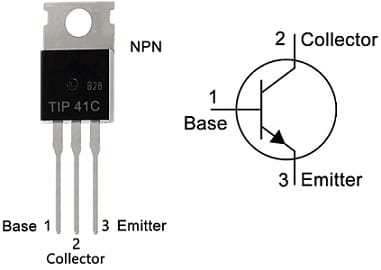
The pin configuration of the TIP41C transistor with the symbol is shown below. The TIP41C transistor includes three terminals; the emitter, base & collector which are discussed below.

TIP41C Transistor Pin Configuration
- Pin1 (Base): The base terminal of this transistor is used to trigger the device.
- Pin2 (Collector): The collector terminal of this transistor allows the flow of current.
- Pin3 (Emitter): The flow of current will exit from this terminal.
Features & Specifications:
The features and specifications of the TIP41C transistor include the following.
- TIP41 is an NPN BJT Transistor.
- The range of DC current gain is 15 – 75hFE.
- Its collector current or IC is 6Amps.
- Its collector to base voltage or VCB is 40Volts.
- Its collector-to-emitter voltage or VCE is 40 Volts.
- Its emitter to base voltage or VEB is 5Volts.
- Its base current or IB is 2Amps.
- Its transition frequency or FT is 3MHz.
- The peak power dissipation is 65 watts.
- TIP41 is an NPN power transistor with a maximum gain of 75.
- Its collector-to-emitter voltage is 100 volts.
- The base current of this transistor is about 3 Amps.
- The emitter to base voltage is 5 volts.
- Its storage temperature ranges from -65 to 150 degrees C.
The complementary TIP41 transistor is the TIP42 transistor. Equivalent & Replacement TIP41 transistors are; BD705, BD709, BD707, BD905, BD909, BD907, BDT41A, BDT41, BDT41AF, BDT41BF, BDT41B, BDT41F, TIP41AG, TIP41A, TIP41B, TIP41G/TIP41BG.
Working
The working of this TIP41C transistor is; when a small input current is used across a single pair of transistor terminals to generate a large current across the remaining pairs of terminals. So this procedure is used mainly for amplification purposes. This transistor controls the low i/p current and generates a high o/p current, so due to this reason, this transistor is known as a current-controlled device. The two charge carriers; electrons & holes are used for the conductivity process. So the major charge carriers in this transistor are electrons & holes are minor charge carriers.
For the action of this transistor, the base terminal is responsible. Whenever a positive (+ve) voltage is provided at the base terminal of this transistor, it gets biased to start the action of the transistor. In this transistor, the flow of current will be from the collector terminal to the emitter. The base pin of this transistor works like a control valve to control the electrons.
12V to 5V Converter Circuit
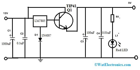
The 12V to 5V converter circuit diagram is shown below. The required components to make this circuit mainly include; LM7805 voltage regulator, Q1-TIP41 NPN transistor, C1-1000 uF, C2-0.1 uF, C3-100 uF, C4-0.01 uF, D1-1N4007, Red LED, R1-330 ohms resistor and 1 heatsink for Q1 transistor. Connect the circuit as per the connections shown below.

12V to 5V Converter Circuit
This 12V to 5V converter circuit is very useful for cars. It can be used to connect 5V electronic devices within a car through a 12V battery. In the circuit, a 5volt LM7805 voltage regulator is used to deliver the maximum 1 amp of current. This 1 amp amount of current is not enough for some devices that we desire to connect. If we connect a minimum of two or more devices at the same time, then this current is not sufficient. This problem can be solved by using a TIP41 NPN transistor to enhance the current within the output.
Working
This 12V to 5V converter circuit delivers sufficient current with the Q1 transistor & 5V voltage regulator as shown in the above circuit diagram. In the above circuit, the two capacitors; C1 & C3 are utilized at the input to level the voltage & the regulator’s output. Similarly, C2 & C4 capacitors are utilized to filter any produced interference through the automotive electrical system.
This converter circuit has one main drawback that is; the voltage drop at the base emitter is 0.6V/0.7V, which causes the o/p voltage to be 4.3/4.4V. So this voltage is dissimilar from the necessary 5V. Due to this reason, a 1N4007 diode is connected simply to the Ground pin of the regulator to balance the voltage drop. A red color LED in this circuit is mainly used to indicate that the voltage regulator is active. The resistor ‘R1’ used in the circuit is a current-limiting resistor. Similarly, for a 12V to 9V converter circuit for a car, a zener diode is used in place of a voltage regulator.
Please refer to this link for Choosing Base Resistance for Transistors in Electronic Circuits.
How to Use TIP41C transistor in a Circuit for a long period ?
To make this transistor stay constant for many years within your application circuits, it is suggested to not drive any load above 6A. Always utilize a suitable heat sink and do not drive any load above 100V. For best performance always operate & store this transistor above -65 degrees centigrade temperature & under +150 degrees centigrade.
TIP41C Transistor Applications
The applications of the TIP41C transistor include the following.
- The TIP41C transistor is used in general-purpose amplification & switching applications.
- This transistor can be used as a switch to drive several loads simultaneously like high-power LEDs, DC motors, bulbs, high-power relays, etc.
- This transistor is used to design a simple high-power amplifier circuit and also in high-power-based audio amplifier stages.
- This transistor is used for audio & signal amplification.
- This transistor drives loads below 6 Amperes.
- This type of transistor is used to drive & control DC Motors
- TIP41C transistor is used in Darlington pairs.
- This transistor is used in different circuits like amplifiers, motor driving, inverter, SMPS & rectifier circuits.
Please refer to this link for Choosing Base Resistance for Transistors in Electronic Circuits.
Please refer to this link for Replacing Transistors in Electronic Circuits.
Please refer to this link for How to Select a Transistor.
Please refer to this link for the TIP41C Transistor Datasheet.
Thus, this is an overview of the TIP41C transistor, pin configuration, specifications, circuit working, and its applications. This is a NPN power transistor with base island technology and this transistor is available in a TO-220 plastic package. This is suitable for power linear, switching & audio applications. The complementary TIP41C NPN transistor is the TIP42C PNP transistor. Here is a question for you, what is TIP42C PNP transistor?