NPN transistor is one type of transistor where one P-type material is sandwiched between two N-type materials. The main function of this NPN transistor is to amplify the weak signal which enters the base terminal & generates a strong signal at the collector terminal. In this type of transistor, the electron movement direction will be from the emitter terminal to the collector. These transistors are mostly used as compared to PNP because electrons are the majority charge carriers in this transistor and they have high mobility. This article provides brief information on the NPN transistor – S9013 transistor, circuit working, and its applications.
What is the S9013 Transistor?
SS9013 is an NPN, fast, and high-current transistor and is available in the TO-92 package. This transistor is frequently used within commercial devices for general-purpose amplification & switching purposes. This NPN transistor has one P and two N regions where N-regions are doped with the electrons and P- region is doped with holes because the majority of current supplies are due to the movement of electrons & holes within this transistor.
This is an epitaxial silicon (Si) planar NPN transistor, used in the audio o/p stage and inverter/ converter circuits. This NPN transistor has an outstanding capability of gain so that it can be used in amplifier applications. This transistor provides a maximum 150 DC gain & it can have 140MHz of frequency. Its maximum collector current is 500mA & collector power dissipation maximum is 625mW.
Pin Configuration:
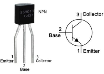
The pin configuration of the S9013 Transistor is shown below. This transistor includes three terminals which are discussed below. The pin diagram of the S9013 Transistor and its symbol are shown below.

S9013 Transistor Pin Configuration
- Pin1 (Emitter): Current supplies out of this emitter terminal
- Pin2 (Base): The flow of current through this terminal will control the current supply between the emitter & collector terminals.
- Pin3 (Collector): Current flows throughout this terminal
Features & Specifications:
The features and specifications of the S9013 transistor include the following.
- It is an NPN-type transistor.
- It includes three terminals.
- The type of package is TO-92.
- Its power dissipation is 650mW.
- Its collector current maximum is 5A/500mA.
- Its collector-to-emitter voltage or VCE is 20 volts.
- Its collector to base voltage or VCB is 40Volts.
- Its emitter to base voltage or VBE is 5Volts.
- Its collector dissipation maximum (Pc) is 625 Milliwatt.
- Its transition frequency maximum (fT) is 150 MHz.
- Its min & max DC current gain or hFE is 64 to 202.
- Its Gain minimum is 40 & maximum is 300.
- The PNP complementary S9013 transistor is SS9012.
- Maximum storage and operating temperature range must be from -55 to +150 degrees Centigrade.
- Alternative or equivalent S9013 transistor is; S9013, 2N4401, S8050, 2N3904, S8050, BC547, 2N2222, BC338, BC337 etc.
12V Switching DC Regulator Circuit using Transistors
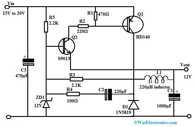
The 12V simple switching power supply circuit with transistors is shown below. At present, switching power supply circuits are designed with ICs due to their high efficiency and convenience. But here the following circuit is designed with two transistors along with a few components. This simple switching regulator circuit is a step-down DC converter that is used to change the 15V to 20V input voltage to the 12V output voltage.
The required components to make this 12V switching DC regulator circuit using transistors mainly include; transistors Q1-BD140 and Q2-S9013, D1-1N5819, schottky barrier diode, 12V 0.5W ZD1- zener diode, electrolytic capacitors; C1-1,000µF 25V, C2-220µF 25V and C3-470µF 35V, 0.25W carbon or metal film resistors; R1-470Ω, R2-220Ω, R3 & R5: 2.2K, R4-100Ω and L1-220µH inductor. Connect the circuit as per the circuit diagram shown below.

12V Switching DC Regulator Circuit with Transistors
Working
The Q1- BD140 transistor in this circuit works as switching where the main components like L1, & D1 are connected to this transistor. In this circuit, both the NPN and PNP transistors work as feedback to each other to produce the frequency or to function as the switching continuously. However, in this circuit diagram, the coil’s current is not the highest because there is a voltage detector (or) error sensor through the R4, C2 & 12V ZD1 Zener diode for controlling the voltage to be stable
Whenever we provide a DC input voltage supply to this circuit, then it will make the Q2 – S9013 transistor acquire a biased current as the current supplies throughout the R5 resistor to bias the Q2 transistor into the current conduction & impact to the transistor Q1.
This Q1 transistor has the flow of current throughout the emitter terminal to the base to transmit the current flow throughout the Q2 conduction. This makes the Q1 transistor apply current supply to the collector terminal to the coil ‘L1’ however, since the Q2 base terminal has a fixed reference ZD1 (Zener diode) to maintain the stable voltage at 12Volts.
Whenever the o/p voltage increases up to 12Volts, then it causes the voltage across the Q2 transistor’s emitter terminal is also high because it is at a similar point. So the result is Q2 transistor turns off, so the Q1 transistor will stop conducting the current also.
How to securely use the S9013 transistor for long run within a circuit?
For long-term & security performance, this transistor must be operated above 20Volts. For the transistor base, a suitable current-limiting resistor is necessary. Always situate the transistor pins in the circuit properly. This transistor should not be connected with above 500mA of load. It should be operated in the range of temperature from >-55 centigrade to < +150 centigrade.
To know more on biasing of the transistor click on the link and to know on how to connect a transistor as a switch click on the link.
Advantages & Disadvantages
The advantages of the S9013 Transistor include the following.
- Its power consumption is low so useful for low-voltage applications.
- It has a high DC current gain so a small current at the base terminal controls a huge collector current.
- The saturation voltage from the collector to the emitter is low.
- These are very small & compact so they can easily incorporated into electronic circuits.
- It occupies less space.
- These are cost-effective.
The disadvantages of the S9013 Transistor include the following.
- Power handling capacity is limited.
- Voltage handling capacity is limited.
- Frequency response is limited.
- It is a polarized device so its terminals should be connected in the exact polarity for its proper operation.
S9013 Transistor Applications
The applications of the S9013 transistor include the following.
- S9013 transistor is used in different electronics applications.
- This transistor’s collector-emitter voltage is 20Volts, so it can be used easily in electronic applications that need below 20Volts.
- This NPN transistor is mainly designed for audio amplification. It can be utilized in circuits wherever around 1W of small audio amplification is necessary like small radios, electronic buzzers, receiver circuits, electronic bells, audio signal amplification of electronic applications, etc.
- This transistor can be used for operating loads such as relays, ICs, high-power LEDs, and electronic applications for switching purposes due to 500mA of collector current.
- It is used in a 1Watt audio amplifier within any electronic application
- Its drives load below 500mA.
- This transistor can be used as a switch & amplifier for electrical signals.
- These can be used in circuits as electrical rectifiers.
- It is used as a switch.
- These transistors are used in high-frequency-based amplifiers, high-current drivers, switching converters, etc.
Please refer to this link for the S9013 Transistor Datasheet.
Thus, this is an overview of the S9013 Transistor, pin configuration, specifications, circuit working advantages, disadvantages, and applications. This is a small NPN bipolar junction transistor used frequently in electronic circuits as a switch or an amplifier. This transistor has less power consumption & a high DC current gain so it is used in low-voltage-based applications. So in the electronics industry, this transistor plays a key role because of its simple use, versatility & low cost. Here is a question for you, what is an S8050 transistor?