We know that there are different types of diodes are used in different applications based on the requirement like Varactor diode, Schottky diode, LED, Zener diode, etc. Even though, the most popular diode including a basic PN- junction is also used in different circuits which are called a PIN diode. As compared with a normal PN junction diode, this kind of diode is different because this diode includes three layers like P, I & N whereas the PN junction diode includes two layers like P & N.
In this diode, there is a pure semiconductor material is available in between two layers P & N that is ‘I’ (intrinsic material of Si & Ge). Here, the two layers like P & N are extremely doped to function like ohmic contact whereas intrinsic layer ‘I’ works as an insulator so there is no flow of current through it. So, the structure of PIN is very useful in RF switching and photodiodes.
What is PIN Diode?
The full form of the PIN diode is, Positive-Intrinsic–Negative. PIN diode can be defined as the diode in which the high resistivity intrinsic layer ‘I’ is arranged in between the two layers of semiconductor material like P & N. In between these two layers, the intrinsic layer provides a high electric field that induces due to the charge carrier’s movement like electrons & holes. Here, the electric field direction will be from N to P-region.
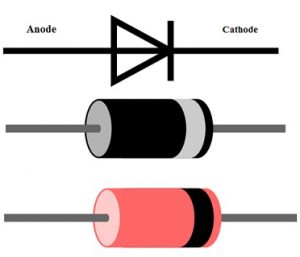
This diode includes two terminals, namely anode, and cathode, known as positive and negative terminals. The symbol of the PIN diode is shown below.

PIN Diode Symbol
The high electric field will produce huge pairs of electron holes because the diode will process even for the tiny signals. This diode is a kind of photodetector that is used to change the energy from light to electrical.
The layer ‘I’ between both the layers of P & N will increase the distance between them. If the distance between the two layers increases then their capacitance will be decreased. The PIN diode characteristic will increase their response time so that it can be used in microwave applications.
PIN Diode Construction
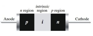
The construction of a PIN diode is shown below. This diode includes three layers like P-layer, an intrinsic layer, an n-layer. Here, the formation of the P-layer can be done through trivalent impurity doping toward the semiconductor. The n region can be formed by doping pentavalent impurity toward the semiconductor material. Here, the intrinsic semiconductor layer is not doped material.

PIN Diode Construction
The formation of PIN diode can be done through two methods namely planar structure otherwise mesa structure. In a planar structure, the A P+ region can be formed through a thin epitaxial layer by forcing it over the intrinsic layer. Likewise, the N+ region can also be formed over another face of the substrate. Here the intrinsic layer gives 0.1 Ω-m which is extremely high resistive. In the mesa structure, the semiconductor layers are doped previously on the intrinsic region. So that PIN diode can be constructed
PIN Diode Working
The working principle of a PIN diode is similar to a PN junction diode but the only difference is the intrinsic region. This region works like a depletion layer in between two layers like P & N. Once no exterior potential is applied to the PIN diode, then charge carriers will disperse across the junction due to the concentration gradient.
Therefore, the depletion region can be formed at NI- junction (N region & intrinsic region). As compared to N-region, the thickness of the ‘I’ region is higher because the n-region doping level is higher as compared to the ‘I’ region
Forward biased Condition
In a forward bias condition, when the voltage is applied to the PIN diode, then charge carriers in both the regions will be injected into the intrinsic layer.
So the applied forward potential will decrease the depletion width. Because of this, the resistance provided by this diode is no biased condition will start decreasing due to forward biasing. So, when the forward voltage is enhanced, a high number of charge carriers will be injected into the intrinsic layer.
Thus, generating a large current through the device will result in decreasing the resistance. Thus, in this biasing condition, this diode works as a variable resistance device.
Reverse Biased Condition
When the reverse bias voltage is supplied to the diode then the depletion width will start rising. When the reverse voltage is raised, then the depletion region width will increase until the carriers move away from the intrinsic layer. So, this specific voltage is called swept out voltage and generally, its value is -2V.
In this biasing, the diode works like a capacitor. Here both the regions like P & N serve like the capacitor’s two plates. In a high reverse bias case, a thin depletion layer can be observed within the P-layer.
PIN Diode Characteristics
The characteristics of the PIN diode include the following.
- Low Capacitance
- High breakdown voltage
- Sensitive to photodetection
- Charge carriers storage
A PIN diode provides less capacitance value because of the distance between two regions. Once a reverse potential is applied to the diode, then the depletion region will completely be depleted. Once this region is depleted, then the capacitance does not demonstrate change through the potential applied because of the small amount of charge within the intrinsic layer.
Because of the intrinsic region, this diode shows a maximum breakdown voltage value which is necessary to wipe out the wide depletion region. The depletion layer is accountable to produce energy once radiation drops on its exterior. The intrinsic region occurrence will improve the region for the absorption of radiation. Therefore, these are extensively used like photodetectors.
The storage of charge carriers will be enhanced through the intrinsic region. The charge which is stored within the depletion region is accountable for the sum of current supply throughout the circuit. Once forward biasing is applies to this diode, the diode will show the characteristics of uneven resistance because the resistance changes through the input voltage applied to it & it does not generate rectification & distortion.
Advantages
The advantages of the PIN diode include the following.
- Less noise
- Frequency response is good
- High reverse voltages to be accepted
- Less dark current
- Linear
- The depletion region is large
- Used as a variable resistance device
- The bias voltage is less
- Junction capacitance is low
- The response speed is high
- Responsive to the light
Disadvantages
The disadvantages of PIN diode include the following.
- Less active area
- Reverse recovery time is high because of power loss
- Response time is not fast
- Less sensitivity
- There is no internal gain
- Temperature-dependent
- In dark current, it increases rapidly
- Needs amplification at less illumination region
Applications
The applications of PIN diode include the following.
- The PIN diode applications involved a wide range like frequency switch, microwave attenuator, radiofrequency attenuator, photodetector, microwave switch, etc
- These kinds of diodes are used for detecting X-rays as well as gamma rays.
- PIN diodes are utilized in the RF, microwave switches, variable attenuators because they have less capacitance.
- These diodes are applicable in photovoltaic cells, Photodetectors, switches, and fiber-optic network cards.
- Used in RF protection circuits, an RF switch, high voltage rectifier, photodetector.
PIN Diode Circuit
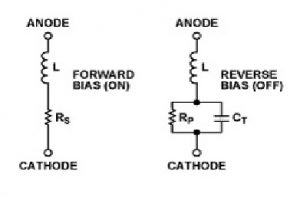
A PIN diode is used like a current-controlled resistor at microwave & RF frequencies. When the diode is forward biased, the resistance can range from a division of an ohm otherwise ON and above 10 kΩ once it is reverse biased otherwise off. Compared to PN junction diodes, these diodes include an extra resistive intrinsic semiconductor material layer between two materials like P-type & N-type. Once a PIN diode is connected in forwarding bias, then majority charge carriers from p-type & N-type are injected into the intrinsic area.

PIN Diode Circuit
These charge carriers cannot recombine immediately; the fixed amount of time necessary for them to recombine is known as the lifetime of the carrier. So this can cause a net stored energy within the intrinsic region, decreasing the resistance value and assigned as RS.
Once the diode is connected in reverse bias, and then the PIN diode will come into view like a large resistance ‘RP’ that is shunted through a CT capacitance. By changing the diode geometry, it is possible to change PIN diodes to have different RS & CT combinations to meet the requirements of different frequency ranges as well as circuit applications.
Know more about Schottky Diode MCQs & Tunnel Diode MCQs.
Please refer to this link for Choosing resistor values for diodes.
Thus, this is all about an overview of PIN Diode and its working with applications. These diodes are used in various fields like RF switch, RF attenuator, microwave switch, photodetector, microwave attenuator, photovoltaic cell, fiber optic network cards, etc. Here is a question for you, what are the different types of PIN diode?