PIC18F2550 is one of the cheapest 8-bit PIC18FXXXX series microcontrollers, designed by MICROCHIP. This series of PIC microcontrollers is very famous because of its cheapness, multiple features & performance. This microcontroller can be directly interfaced with the other personal computer. This is a very popular microcontroller, so most of the engineers and developers use it. This PIC microcontroller keeps the peripheral still active whenever the CPU core is on standby & utilization of the internal oscillator leads the controller to conserve up to 90% power saving. This PIC18F2550 microcontroller is promoted further by adding several features together. This article provides brief information on the PIC18f2550 microcontroller, pinout, specifications, and its applications.
What is the PIC18f2550 Microcontroller?
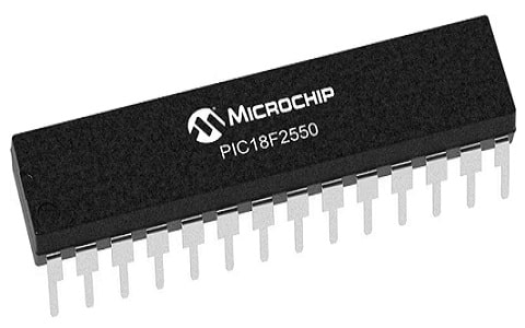
PIC18F2550 PIC microcontroller is one of the cost microcontrollers available in the market to work with a lot of tutorials and also has support on the Internet to assist beginners. This microcontroller has flash memory -32Kbytes which is sufficient for several applications.
PIC18f2550 microcontroller has 24 programmable I/O pins which can interface easily with many peripherals. This microcontroller can be utilized on systems without human interference using a Watchdog timer to reset in error automatically. This microcontroller has a USB interface feature which is very helpful in communicating with a controller from any personal computer without any bother.

PIC18f2550 Microcontroller
Working
PIC18F2550 microcontroller works like any other type of PIC microcontroller but, microcontrollers are not similar to digital ICs because they need power to work whereas Microcontroller works with the program before getting the IC working. Thus, for the functioning of the PIC18F2550 microcontroller, we need to save the right program file first within the FLASH memory of the microcontroller. Whenever power is given to the microcontroller, it executes saved code within FLASH memory to generate the response.
PIC18f2550 Microcontroller Pin Configuration:
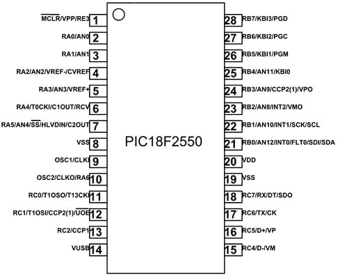
The pin configuration of the PIC18f2550 microcontroller is shown below. This microcontroller includes 28 pins which are discussed below.

Pin Configuration
Pin1 (MCLR/VPP/RE3):
- MCLR is a Master Clear or RESET Input pin.
- VPP is a programming voltage input pin.
- RE3 is the I/O pin of PORT-E.
Pin2 (RA0/AN0):
- RA0 is an I/O pin of PORT-A.
- AN0 is an analog input-0.
Pin3 (RA1/AN1):
- RA1 is an I/O pin of PORT-A.
- AN1 is an analog input-1.
Pin4 (RA2/AN2/VREF-/CVREF):
- RA2 is an I/O pin of PORT-A.
- AN2 is an analog input-2.
- VREF- is an A/D reference low voltage input pin.
- CVREF is an analog comparator reference output pin.
Pin5 (RA3/AN3/VREF+):
- RA3 is an I/O pin of PORT-A.
- AN3 is an analog input-3 pin.
- VREF+ is an A/D reference high voltage input pin.
Pin6 (RA4/T0CKI/C1OUT/RCV):
- RA4 is an I/O pin of PORT-A.
- T0CKI is a Timer-0 external CLK input.
- C1OUT is an output of a comparator-1.
- RCV is an external RCV input of a USB transceiver.
Pin7 (RA5/AN4/SS/HLVDIN/C2OUT):
- RA5 is an I/O pin of PORT-A.
- AN4 is an analog input-4.
- SS is SPI slave select input.
- HLDVIN is high/low-voltage detect input.
- C2OUT is an output of comparator-2.
Pin8 (VSS): It is a ground pin.
Pin9 (OSC1/CLKI):
- OSC1 is an Oscillator pin-1.
- CLKI is an external CLK source input pin.
Pin10 (OSC2/CLKO/RA6):
- OSC2 is an oscillator pin-2
- CLKO is a CLK source output pin.
- RA6 is an I/O pin of PORT-A.
Pin11 (RC0/T1OSO/T13CKI):
- RC0 is an I/O pin of PORT-C.
- T1OSO is the Timer-1 oscillator output pin.
- T13CKI is Timer1 or Timer3 external CLK input pin.
Pin12 (RC1/T1OSI/CCP2/UOE):
- RC1 is an I/O pin of PORT-C.
- T1OSI is a Timer-1 oscillator input pin.
- CCP2 is a capture-2 input or Compare-2 output or PWM2 output.
- UOE is an external OE output pin of a USB transceiver.
Pin13 (RC2/CCP1):
- RC2 is an I/O pin of PORT-C.
- CCP1 is capture-1 input or Compare-1 output or PWM1 output.
Pin 14 (VUSB): It is an internal voltage regulator USB 3.3V output pin.
Pin15 (RC4/D-/VM):
- RC4 is an I/O pin of PORT-C.
- D is differential minus the line of USB.
- VM is a VM input of an external USB transceiver.
Pin 16 (RC5/D+/VP):
- RC5 is an I/O pin of PORT-C.
- D+ is a USB differential plus line.
- VP is the VP input of an external USB transceiver.
Pin17 (RC6/TX/CK):
- RC6 is an I/O pin of PORT-C.
- TX is an asynchronous transmit pin of EUSART.
CK is synchronous CLK of EUSART.
Pin18 (RC7/RX/DT/SDO):
- RC7 is an I/O pin of PORT-C.
- RX: is an asynchronous receive pin of EUSART.
- DT is the synchronous data pin of EUSART.
- SDO is SPI data out pin.
Pin19 (VSS): It is a GND pin.
Pin20 (VDD): It is a +5V positive power supply pin.
Pin21 (RB0/AN12/INT0/FLT0/SDI/SDA):
- RB0 is an I/O pin of PORT-B.
- AN12 is an analog input-12 pin.
- INT0 is an external interrupt-0 pin.
- FLT0 is an enhanced PWM fault input pin.
- SDI is SPI data in pin.
- SDA is an I2C data I/O pin.
Pin22 (RB1/AN10/INT1/SCK/SCL):
- RB1 is an I/O pin of PORT-B.
- AN10 is an analog input-10 pin.
- INT1 is an external interrupt-1 pin.
- SCK is a synchronous serial CLK I/O for SPI mode.
- SCL is a synchronous serial CLK I/O for I2C mode.
Pin23 (RB2/AN8/INT2/VMO):
- RB2 is an I/O pin of PORT-B.
- AN8 is an analog input-8 pin.
- INT2 is an external interrupt-2 pin.
- VMO is an external VMO output of a USB transceiver.
Pin 24 (RB3/AN9/CCP2/VPO):
- RB3 is an I/O pin of PORT-B.
- AN9 is an analog input-9 pin.
- CCP2 is a capture-2 input or compare-2 output or output of PWM2.
- VPO is the VPO output of an external USB transceiver.
Pin25 (RB4/AN11/KBI0):
- RB4 is an I/O pin of PORT-B.
- AN11 is an analog input-11 pin.
- KBI0 is an interrupt-on-change pin.
Pin26 (RB5/KBI1/PGM):
- RB5 is an I/O pin of PORT-B.
- KBI1 is an interrupt-on-change pin.
- PGM is a low-voltage ICSP programming enable pin.
Pin 27 (RB6/KBI2/PGC):
- RB6 is an I/O PORT-B pin.
- KBI2 is an interrupt-on-change pin.
- PGC is an In-Circuit debugger & ICSP programming CLK pin.
Pin28 (RB7/KBI3/PGD):
- RB7 is an I/O pin of PORT-B.
- KBI3 is an interrupt-on-change pin.
- PGD is an In-Circuit debugger & programming data pin of ICSP.
Features & Specifications:
The features and specifications of the PIC18f2550 microcontroller include the following.
- PIC18f2550 is a 28-pin PIC microcontroller.
- Its operating voltage ranges from +4.0 to +5.5V.
- This microcontroller is an 8-bit CPU.
- It has 24-programmable I/O pins.
- It has communication Interfaces like the following.
- USB Serial Interface – 15 and 16 pins are used mainly for programming this microcontroller.
- Master/Slave SPI Serial Interface – 7, 18, 21 & 22 pins are used for programming this microcontroller.
Programmable Serial UAR – 17 & 18-pins are used for programming this microcontroller. - Two-wire Serial Interface – 21 & 22 pins are used for connecting peripheral devices such as; LCDs & sensors.
- It has 8-bit counter-1, and 16-bit counters -3.
- It has 10 channels and a 10-bit resolution ADC module.
- It has 2-PWM channels.
- It has 2 – analog comparators.
- It has a 32KHz to 8MHz Internal Oscillator.
- This microcontroller has up to 48MHz external oscillator.
- The program memory type is Flash.
- It has power-saving modes.
- RAM is 2K bytes.
- Program memory / Flash memory is 32K bytes.
- EEPROM memory is 256Bytes
- Its CPU Speed is 12 MIPS.
- It has a programmable watchdog timer including a separate On-chip Oscillator.
- Operating temperature ranges from 40°C to +85°C.
PIC18F2550 Programming
To learn PIC microcontroller programming, one should have a grip on GPIO pins. To program this microcontroller, you can utilize either c programming or assembly language to program.
The following steps need to be followed for PIC18F2550 microcontroller programming.
- The first step is, that the functions need to be executed with a microcontroller.
- Those functions must be written in ‘IDE software’ with a supported programming language.
- Once the desired program is written then compile using IDE for removing errors.
- After compilation is done successfully, the IDE application provides a HEX file mainly for the written program.
- Select the programming device to establish the communication between the PC & microcontroller.
- After that, need to run the HEX file-dumping software which is related to the selected programming device.
- Select the suitable program HEX file.
- Burn the HEX file within the flash memory of the microcontroller using this program.
- Disconnect the programmer & connect the suitable peripherals for the microcontroller.
Tools
There are different tools are used for microcontroller programming. To begin with microcontroller programming, the following software & hardware components are required.
A Compiler/IDE to Write a Program within C Language (or) Assembly:
A compiler is an integrated development environment where you type your primary microcontroller program. It is used to produce a hex file which is uploaded to a microcontroller by a user. There are three most famous compilers used for microcontroller programming; Mikro C, MPLABX IDE for PIC & PIC CCS compiler.
Programmer/Burner:
Once you finish writing your code, then you have a hex file that you are required to upload into a PIC microcontroller. So, a programmer (or) burner is useful in uploading binary files into the microcontroller. For code burning, Pickit3 is the best choice.
PIC Development Boards:
These boards are non-compulsory however they make your development procedure very simple because they provide many onboard peripherals such as; Sensors, ADCs, GPIO connectors, etc.
PIC18F2550 Microcontroller Architecture
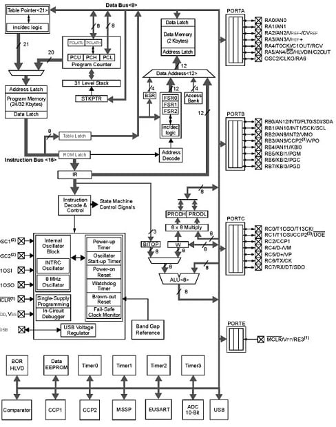
The PIC18f2550 microcontroller architecture diagram is shown below which includes different blocks that are discussed below.

PIC18f2550 Microcontroller Architecture
GPIO Ports
This PIC microcontroller includes four GPIO ports which include digital pins like Port-A, Port-B, Port-C, and Port-E). Except for Port-E, the remaining three ports provide the o/p function. The output pin connects to the port-A & B which provides the TTL logic although the output of port-c is available in ST logic. The GPIO pins on this microcontroller are RA0 to RA6, RB0 to RB7 & RC0 to RC7.
Digital i/p Pins
Every port in this microcontroller includes digital input pins. In ports A & B, all the input pins are operated through TTL input although port C, operates with TTL input only and other pins on ports C & E need ST logic to operate or else it could cause trouble for the program of the microcontroller to know & operate correctly. Digital i/p pins includes RA0 to RA6, RB0 to RB7 & RC0 to RC7.
Interrupts
Each external device needs to interrupt function while getting the notice of CPU & microcontroller has 3-interrupts which can be utilized to get the input signal to produce the interrupt in the microcontroller. Interrupts are INT0 to IN2.
EUSART Asynchronous
Most of the systems need serial communication systems & the Eusart Asynchronous serial communication system is a very popular system used for serial communication. This includes separate data transmitting & receiving pins (TX and RX) and both can be utilized simultaneously.
SPI Communication
This controller needs external modules sometimes to achieve communication & some of them utilize the SPI communication technique which is known as a three-wire communication system. This system utilizes two data wires, a single CLK pulse wire & a slave select, used in multiple peripherals. SPI pins mainly include; SDO, SDI, SCK & SS.
I2C Communication
I2C is a 2-wire serial communication although it is single-way. This communication utilizes two wires where one wire is used for CLK pulse & remaining wire is used for transmitting & receiving data. In this communication, the CLK signal assists the microcontroller to utilize several peripherals simultaneously. I2C pins of this communication mainly include SDA & SCL.
EUSART Synchronous
The controller IC has several methods to program although it can be programmed with synchronous serial programming. Here three pins are used to program the controller serially like first pin is used for the CLK, the second is for data transmit/receive & third pin is used for programming power input. These pins mainly include; VPP, CK & DT.
ICSP Serial Programming
ICSP is in-circuit serial programming that utilizes a special programming circuit, designed by the MICROCHIP Company to program the PIC microcontroller with the HEX file of the program. So in this procedure, there are six pins are used; MCLR, VDD, VSS, PGM, PGC & PGD.
USB Communication
The USB in this microcontroller can be directly connected to the PIC microcontroller which includes a half-speed & full-speed USB interface. Here, the USB is connected to the internal or external transceiver. So the internal transceiver is allied to the external USB interface however it also can use the external transceiver when required. The pins for external transceivers mainly include; RCV, VMO, VPO, UOE, VM, and VP – GPIO16. Similarly, the pins for internal transceivers mainly include; VUSB, D+ & D-.
Timers
This microcontroller includes four-timers like; Timer0 with 8-bits & Timer1, 2 & 3 are of 16-bits. The Timer1 in this microcontroller uses the external oscillator which is separate from the oscillator of the PIC microcontroller. Timers 1 & 3 can be operated with exterior input signal and the Time0 & 2 operate internally only: The timer pins mainly include; T0CKI, T1OSO, T13CKI & T1OSI.
HLVDIN
HLVDIN (GPIO7) is a safety-providing pin for the PIC controller which is used to initialize the voltage range in the microcontroller from wherever the device will be trip off. So the input over this pin is an analog input signal which generates the interrupt.
ADC
ADC of this microcontroller is used to convert the signal from analog to digital. In this microcontroller, there are a total of 10 A/D converting channels with 10 bits. All these channels are very useful in converting 10 analog to a digital signal. After this, it stores or uses it based on the instructions provided within the program. This microcontroller has ADC pins which range from AN0-AN12.
VREF
The ADC in this microcontroller is smart due to VREF pins. This microcontroller includes two Vref pins which are used for describing the maximum input voltage of analog signal & minimum input voltage of analog input signal. In this manner, the ADC provides only the output of values in the range provided by VREF. Here, the voltage reference pins mainly include; VREF+ & VREF-.
Comparator
PIC18f2550 microcontroller includes two comparators which are used for comparing several inputs. The inputs can be any analog input signal taken from AN0 to AN4 and the output voltage is compared on the VDD. Comparator pins include; CVREF, CV1OUT, and CV2OUT.
CAPTURE or COMPARE or PWM Module
This microcontroller has two capture or compare or PWM pins. So this internal module utilizes Timers 1 and 3 that allow the device to produce the output at a particular time. So this module simply allows the microcontroller to produce PWM of the preferred duty cycle with timers & Prescaler. This module’s output pins mainly include; CCP1, CCP2/RC1, CCP2/RB3, and FLT0.
RB3 pin gives the output by default, however, RC1 & RB3 can be distinguished internally from the program. Here, a fault detection pin is utilized to initialize the least fault active period in CCP1.
RESET Pins
PIC18F2550 microcontroller includes an external reset pin (MCLR), used to reset the microcontroller. This is an active low pin, operated with a button (or) some ST logic state device.
Power Input
This microcontroller has three power input pins where one pin is used for power input & the remaining two pins are ground used for making the common GND. They are very common in the microcontroller. The power & ground pins of this microcontroller are; VSS & VDD.
Oscillator or CLK Pins
Each microcontroller needs a CLK signal to operate which is available with an internal CLK from 32 KHz – 8 MHz. It can be adjusted at a different level throughout instructions. To utilize the CLK up to 48MHz, the microcontroller provides two CLK input pins used for input & output. These pins are; OSC1/CLKI & OSC2/CLKO.
PIC18f2550 Microcontroller Interfacing with LDR
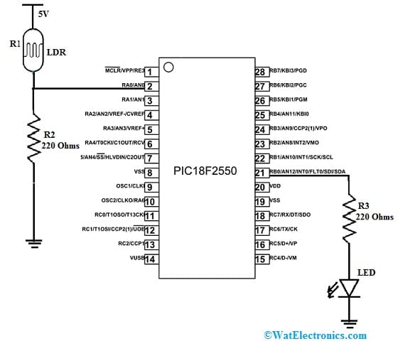
PIC18f2550 Microcontroller Interfacing with LDR is shown below. This circuit is used to activate a light when it is dark. The required components for this interfacing mainly include; an LDR, 5V Supply, PIC18f2550 Microcontroller, 633 Ohm RED LED, and R2 & R3 220 Ohms – Resistors.

PIC18f2550 Microcontroller Interfacing with LDR
The connections of this interfacing follow as;
- LDR one terminal is connected to 5V Supply and the other terminal is connected to pin-2 of PIC18f2550 microcontroller.
- R2 220 Ohms resistor one terminal is connected to LDR one terminal and pin-2 of the microcontroller. The other terminal of this resistor is connected to GND.
- 633 Ohm RED LED positive terminal is connected to pin-21 of the microcontroller through an R3 220 Ohms resistor. The other terminal of this LED is connected to GND.
Code:
The required code for this interfacing is given below which is written in mikroC Pro for PIC18f2550 microcontroller.
#include <built_in.h> // Built-in library for mikroC
void main() {
// Initialize the ADC
ADCON1 = 0x0E; // Configure AN0 (RA0/AN0) as analog input, rest as digital
ADCON2 = 0xA9; // Right justified, 16 TAD, Fosc/8
ADCON0 = 0x01; // Enable ADC and select channel AN0 (RA0)
TRISA = 0xFF; // Set PORTA as input
while (1) {
// Start ADC conversion
ADCON0.GO_DONE = 1;
while (ADCON0.GO_DONE); // Wait for the conversion to finish
// Read ADC result
unsigned int adcValue = (ADRESH << 8) + ADRESL;
// Convert ADC value to a voltage (assuming Vref = 5V)
float voltage = adcValue * 5.0 / 1023.0;
// Process the voltage value as needed
// For example, you can implement your own logic based on the LDR reading
// Here, we are just demonstrating a delay based on the LDR value
Delay_ms((unsigned int)(voltage * 100)); // Example delay
}
}
Working
A dark-activated light concept is very simple and uses an LDR to an ADC pin on our PIC micro, after that we read in a value depending on the light amount on the light-dependent resistor.
Explanation:
- Configuration settings: These are unchanged from the previous example as they are specific to your hardware setup. Ensure these match your specific configuration.
- Initialization:
- ADCON1 = 0x0E; configures the analog inputs. Here, AN0 (RA0) is set as an analog input, and the rest are digital.
- ADCON2 = 0xA9; sets the ADC conversion clock and acquisition time. 0xA9 is for right justified, 16 TAD, and Fosc/8.
- Main loop:
- Starts the ADC conversion on AN0.
- Waits for the conversion to finish.
- Reads the ADC result from ADRESH and ADRESL.
- Converts the ADC result to a voltage value.
- An example delay function is used to show how to utilize the voltage value (this is just an example, and you can replace it with your logic).
Note:
- Ensure that the ADC channel selection (AN0 in this case) matches the pin you connected the LDR to.
- Adjust the ADCON1 and ADCON2 settings based on your specific requirements and clock speed.
- The delay function used here is for demonstration; in a real application, you might want to perform some meaningful action based on the LDR readings.
This should provide you with the required template to interface an LDR with RA0/AN0 on a PIC18F2550 using mikroC Pro. Adjust the code as necessary to fit your specific project needs.
Advantages & Disadvantages
The advantages of the PIC18f2550 microcontroller include the following.
- PIC18f2550 microcontroller provides many benefits like; high computational performance at a cheap price with an addition of high endurance and enhanced flash program memory.
- These microcontrollers are software-controlled, thus they are similar to small computers.
- It is perfect for low-power & connectivity-based applications that advantage of the accessibility of three main serial ports like; I²C™ & SPI™, FS-USB an asynchronous serial port.
- This microcontroller is very popular because of its multiple features, cheapness, and performance.
- It can interface with any other PC directly.
- This is a very high-performance flash USB Microcontroller including nanoWatt technology.
- PIC microcontroller delivers performance in an order of higher magnitude as compared to its competitors within a similar price category.
- It uses less power which makes it the perfect choice mainly for embedded applications.
- This microcontroller has a large amount of RAM which makes it perfect for embedded monitoring & control applications that need periodic connection with a PC through USB for data & firmware updates
The disadvantages of the PIC18f2550 microcontroller include the following.
- Learning how to write a required program is significant.
- The program & data memory abilities are limited.
- The stack is tiny & the interrupt arrangement is primitive.
- The Input/Output pin has no output ability whenever it is at a high range.
- The program length will be big due to RISC.
- Program memory cannot be accessible & a single accumulator is only present.
Applications
The applications of the PIC18f2550 microcontroller include the following.
- The PIC18F2550 is a versatile & highly capable PIC microcontroller that meets various embedded application demands.
- This microcontroller provides a solid foundation for developers & engineers who looking for a dependable solution mainly for their projects due to its powerful features.
- It can be used with some devices which require an interface through a PC.
- This microcontroller is used in most smart applications because it fills nearly all the communication protocols.
- PIC microcontroller is perfect for low-power & connectivity applications that gain from the accessibility of three serial ports; FS-USB, I²C™ & SPI™.
- PIC18F2550 Microcontroller can be utilized effectively in a wide range of industrial applications.
- This microcontroller is perfect for developing USB peripherals because of its in-built USB interface such as; USB-to-serial converters, USB-enabled input devices & data loggers.
- It can be used within consumer electronics projects which include; smart home devices, remote controls & multimedia controllers.
- This microcontroller is used in industrial automation systems due to its robust feature set wherever it can control sensors, communication interfaces & machinery in manufacturing plants & factories.
- PIC microcontroller is a good choice for different medical devices like; portable diagnostic equipment, infusion pumps & patient monitors because of its accurate communication & ADC capabilities.
- It is used widely in embedded systems for home appliance monitoring & controlling, security systems & automotive applications.
- The PIC18F2550 microcontroller can work as the brain for robotic systems, and sensors, enabling exact control of motors, and actuators within different robotic applications.
- It is used in IoT nodes & sensor platforms which allows data collection & communication through cloud platforms in IoT applications.
- This microcontroller is very popular for educational purposes for helping students & hobbyists learn electronics & microcontroller programming.
- ADC & communication interfaces of this microcontroller are precious for testing, in research, data acquisition systems & scientific instrumentation.
Please refer to this link for the PIC18f2550 Microcontroller Datasheet.
Thus, this is an overview of the PIC18f2550 microcontroller from the PIC18 series, used in high complex, high-density, and high-pin-count applications. This series of PIC microcontrollers provide cost-efficient solutions mainly for general-purpose applications written within C that utilize an RTOS & need a complex communication protocol stack like; CAN, TCP/IP, USB (or) ZigBee. These series microcontroller devices provide flash program memory from 8 to 128Kbytes sizes & from 256 to 4Kbytes data memory and operate at 2.0 – 5.0 voltage range at DC to 40MHz speeds. Here is a question for you, what is the PIC18F4550 Microcontroller?