A p-n junction formed by the doping f p-type and n-type material on a single crystal. The basic device formed from this p-n junction is of two terminals. This is referred to as the p-n junction diode. It is a basic semiconductor device that allows the flow of current in a unified direction. Either germanium or silicon is used as the semiconductor for the purpose of the formation of the diode. Once the voltage is provided to the p-n junction it is termed as biasing of the diode. It can be operated in forward bias as well as in reverse bias. As the voltage is applied the characteristics of the diode are non-linear and it behaves in an exponential way with respect to the applied voltage and generated current in the circuit. The above are some of the basics of the PN junction diode and this article covers about the VI characteristics of the P-N Junction Diode.
VI Characteristics of the P-N Junction Diode
There is the presence of carriers at the junction. The potential developed across the junction due to the influence of the carriers is termed as diffusion voltage. It can be represented as

diffusion-voltage
Because of the potential across the junction, a barrier is formed so that further movement of the carriers can be noticed. This movement in the depletion region is dependent on the applied voltage. This reflects the width of the depletion region. Poisson’s equation determines the relation of the width of the depletion region and the bias voltage.

poisson’s-equation
Here V represents the biasing voltage and ε represents the permittivity of the given semiconductor.
Once the voltage applied there is some amount of current generated in the circuit. It is represented as

generated-current
Here in the above equation, I_s represents the saturation current, where V is the biasing voltage and I the total current generated. Whereas k is the Boltzmann constant e is the charge on the electron and T is the temperature in the Kelvin scale.
Here the biasing voltage, width of the depletion region based on biasing and the current generated in the circuit are related to the general characteristics of the pn junction diode.
Zero Biased Condition in P-N Junction Diode
Zero bias is the condition of the diode without any external supply. Under the unbiased condition, the diode consists of both p-type and n-type semiconductor material and the process of diffusion takes place. This recombination leads to the formation of the electric field. As the electric field is formed it tends to oppose the further movement in the charge carriers. The region formed in between is termed as the depletion region. This leads to the formation of thermal equilibrium state in p-n junction diode.
P-N Junction Diode in Forward Bias
The diode is said to be in forward bias when the p-type is connected to the positive terminal and the n-type is connected to the negative supply of the supply. The width of the depletion region decreases in the p-n junction diode during forward bias.
The VI Characteristics of the PN Junction Diode in Forward Bias
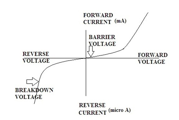
In forward bias condition, the diode gets enough voltage so that it can exceed the value of threshold voltage and provides the carriers with sufficient energy so that it can overcome barrier potential. Hence the forward current is generated in the circuit. The diode tends to conduct once the threshold is crossed.
P-N Junction Diode in Reverse Bias
Once the p-type is connected to the negative terminal of the battery and the n-type is connected to the positive side of the supply the diode is said to be in reverse bias. The width of the depletion region is more in reverse bias of the p-n junction diode.
Please refer to this link for Choosing resistor values for diodes.
The VI Characteristics of the PN Junction Diode in Reverse Bias
Due to minority carriers, there is some generation of the leakage current in the circuit. After some excess reverse voltage, the diode tends to conduct for some time and undergoes breakdown condition. This type of current generated is referred to as Reverse Saturation Current. As the reverse voltage brings sudden changes in the current is termed as Reverse Breakdown Voltage.

V-I Characteristics of P-N Junction Diode
The above are the basics of the p-n junction diode. The voltage and current characteristics are well suited for the explanation of the functioning of the circuit. The circuit can be analyzed better and analysis becomes simpler. The functioning is evident but have you ever given a thought what are the devices that only functions either in forward bias or in reverse bias?