The fundamental unit that evolved because of the same crystal added with acceptor and donor impurities on it. This is highly beneficial because of its features paved the way for the development of modern electronics. This device consists of two terminals but the flow of current will be in a unified direction. The characteristic of this device is tested between the applied voltage and the way current generated in the circuit reacts to it. It can’t be linear but one can determine the relationship between the applied voltage and the circuit current is exponential. This article discusses about P-N Junction Diode theory its Biasing, Forward Bias & Reverse Bias.
Define P-N Junction Diode
A piece of semiconductor with two terminals is referred to as the word Diode. One side of the terminal is added with acceptor impurity and the other is doped accordingly with donor impurity. It is clearly evident that one side is p-type and the other end will be n-type. Hence this type of semiconductor is known as p-n junction diode. The main purpose o this type of device is to facilitate the flow of current in a single direction.
Symbol Representing P-N Junction Diode
The symbol has been designed in such a way that it has an arrowhead pointing in the direction showcasing the flow of direction of the current. A diode consists of two terminals one side of the terminal is known as anode and another side is for the representation of the cathode.
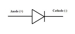
P-N Junction Diode Symbol
P-N Junction Diode Theory
A diode has two regions that are p-type and n-type where it is operated. But on the condition of the applied voltage, the biasing conditions are classified into three types.
Zero Bias
The condition of the p-n junction diode where the device doesn’t have any external supply is known as Zero bias or Unbiased.
Forward Bias
When the positive side of the supply is connected to the p-type and n-type is connected to the negative side of the supply. This bias condition is known as forward bias.
Reverse Bias
When the negative side of the supply is connected to the p-type and the n-type is connected to the positive side of the supply. This type of bias is known as reverse bias.
Working of P-N Junction Diode-type
P-N junction diode working is completely based on the type of bias as well as the p and n-types interact with each other. In p-type the majority carriers are holes and the minority concentration is of electrons. Whereas in n-type the majority of charge carriers will be electrons and the minority of the carriers will be holes.
Basing on the type of bias the diode working can be explained as follows:
P-N Junction Diode under Zero Bias Condition
Zero bias is the condition of thermal equilibrium where the number of charge carriers on both the ends is balanced. As there is no external power supply to the diode the electrons diffuse towards p-side and the diffusion of holes is towards n-side resulting in the generation of the electric field because of these charge carriers diffusion. This generated electric field generated by both the carriers tends to oppose each other. Further, there is no movement of the charge carriers in the depletion region. In this way, the diode is worked under zero bias in order to attain the state of thermal equilibrium.
P-N Junction Diode Working in Forward Bias
This is the condition in which the p-n junction diode is provided with positive supply because the p-type is connected to the positive terminal of the supply. As there is some majority of charge carriers concentration on both the sides tends to attract at the junction resulting in a decrease of the width of the depletion region. This condition results in the establishment of a low impedance path where the high amount of current flows in the circuit.
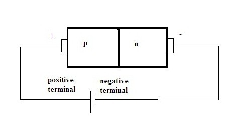
P-N Junction Diode Working in Forward Bias
P-N Junction Diode Working in Reverse Bias
When the p-type is connected to the negative terminal and the n-type is connected to the positive terminal of the supply leads to the condition of reverse bias. As the condition is established the holes in p-type gets distracted from the junction because the p-type is connected to the negative terminal. The same condition is inferred to the electrons in n-type as it is connected to the positive side of the battery and the charged ions left behind during this process. This condition tends to increase the width of the depletion region. Hence the diode becomes completely resistive to the flow of current. In this way, the diode works during reverse bias.
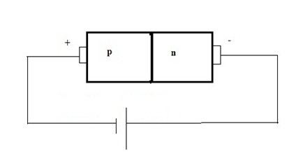
P-N Junction Diode Working in Reverse Bias
How Voltage and Current are Affected in Various Biasing Conditions?
When the curve is plotted between the voltage across the junction and that influences the flow of charged particles that results in the generation of current in the circuit. This voltage and current curve give the characteristics of the p-n junction formed. The respective voltage and current values get influenced by biasing conditions so based on biasing its characteristics varies
Under Zero Bias
In this type of bias, there is no external supply as there is the presence of barrier potential in this condition no carriers are in the movement because the condition of equilibrium is attained. Then the current flowing through the circuit is zero. Because the external voltage applied is zero.
V-I under forward bias
Once the p-n junction is in forward bias it means that forward voltages are applied. Due to this forward biasing the depletion region present at the junction its width tends to decrease. As the width decreases the impedance becomes low and the path established allows high currents to flow.
The point from which there is a sudden increment in the flow of current is termed as knee point. In forward bias, the flow of current through the junction and its magnitude is completely dependent on the supplied voltage.
The approximated current equation when the junction is in forwarding bias is

Current Equation
Here Is represents the saturation current; VT is the volt-equivalent temperature, and n is the emission coefficient.
V-I under Reverse Bias
Generally, in the reverse bias, the p-n junction will be offering the highest resistance to the flow of current. Still, some amount of leakage current flows through the junction. When the reverse voltage applied is of maximum value then the junction gets overheated due to which the breakdown condition occurs and a maximum flow of current is recognized in the circuit.
There is a very tiny amount of current is flowing through the junction as it is in reverse bias. Hence the equation for it is given as

Equation for Tiny Amount of Current
Whereas Is represents the saturation current; VT is the volt-equivalent temperature, and n is the emission coefficient.
Experimental Analysis of P-N Junction Diode
The analysis of the p-n junction diode can be done easily by considering it as a switch. This application of the diode is considered for the experimental setup because of its both biasing conditions execution.
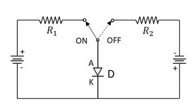
Experimental Analysis of P-N Junction Diode
The biasing conditions of p-n junction’s diode clearly state that during forward bias the diode is in conducting mode acting like a closed circuit. Whereas during reverse bias the diode is in non-conducting or acting as an open circuit. This paved the way the diode to act as a switch. The switch is on during forward bias that is conducting and during reverse bias the switch will be off indicating that it is in non-conducting mode.
Energy Band Diagram of P-N Junction Diode
Energy bands are affected based on the biasing techniques applied. The Fermi levels vary when the diode is unbiased as well as it is forward biased or reverse biased.
Energy Band of Unbiased Diode
When the diode is unbiased the state of the junction will be at equilibrium. It indicates that there is no movement in the charge carriers because both p-type and n-type are at the neutral condition.
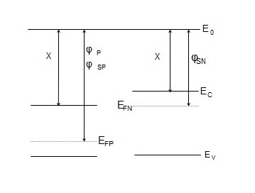
Energy Band of Unbiased Diode
Energy Band of Forward Biased Diode
During the forward bias condition, the p-type is connected to the positive side so that it is convenient for the movement of electrons to flow across the junction in order to combine with the vacancy present there near to the junction.
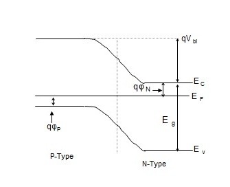
Energy Band of Reverse Biased Diode
Energy Band of Reverse Biased Diode
As the diode is in reverse bias it reflects the condition in energy band where the p-side is supplied with negative voltages that reduces the conduction.
Parameters of P-N Junction Diode
The parameters in the p-n junction diode are as follows:
Reverse Saturation Current – when the p-n junction diode is in reverse bias few amounts of current tends to flow through the diode this is because of the influence of minority charge carriers in it. This is defined as the reverse saturation current.
Barrier Voltage – The voltage that is responsible for the opposing of the flow of majority carriers at the p-n junction from both sides that is p-type as well as n-type is known as barrier voltage.
Reverse Breakdown Voltage – The basic minimum voltage applied to the diode when it is in reverse bias so that the behavior of the diode will change from insulator to conductor for some period of time is defined as the reverse breakdown voltage. The above are some of the parameters of the p-n junction diode.
Please refer to this link for Choosing resistor values for diodes.
Applications of P-N Junction Diode
- The p-n junction diode working under forward bias is very useful for the light emitting diode application.
- The p-n junction diode during the reverse bias is highly sensitive to the light so that it can be used in photodiode application.
- P-N junction during forward bias offers low impedance path whereas during reverse bias acts as an insulator. This process is known as Rectification. Hence p-n junction diode can be used as a Rectifier.
- For the purpose of DC restoration, the diodes are preferably used in clamping circuits.
- These diodes are also utilized in voltage regulation as well as voltage multipliers.
- The above mentioned are some of the uses of the p-n junction diodes.
This is all about the p-n junction diode. As it is like a base for modern electronics this concept is utilized in various applications. It’s been used for LED application as well. But for led’s have you ever thought it is operated in which bias?