Digital logic, the most prominent term which we are aware of today required the cooperation and support of hundreds and thousands of people over many years and decades. Before the invention of electronic devices, mathematicians were inadvertently developing binary logic and laying the basis for current-day computing equipment. These approaches were later employed for the same kind of communication systems such as Morse code and binary. In order to automate the mechanical devices, Charles Babbage and George Boole applied these approaches. Later with many innovations and inventions, logic gates were developed which were in use today on a prominent basis. This article helps us in understanding the concepts of NOR gate definition, circuit, design, applications, and its advantages.
What is NOR Gate?
NOR gate also called Negated OR. NOT OR is the combination of OR and NOT gates which are in series connection. The Negated OR gate is one of the universal logic gates because with the universal gates any other fundamental operations can be accomplished. Therefore, the combination of NOR and NAND gates can give AND, OR, and NOT gates.
Negated OR gate gives the output LOW when both the inputs are at logic LOW or when either of the inputs is at a logic LOW state. The output is HIGH only when both the inputs are LOW.
The NOR gate Boolean expression is given by:
A = (X + Y)’
Here, X and Y are the inputs and A is the output. NOR logic gate can be achieved by adding all the inputs and then completing the obtained result.
The NOR gate symbol is shown as follows:
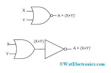
Basic NOR Gate
NOT-OR Gate Types
There are basically three types of NOR logic gates depending on the number of inputs. Those are explained below:
2-input NOT OR
Here, the gate accepts two inputs and gives a single output which is the basic form of NOR gate. Here, the total possible combinations of inputs are 4. The 2-input Negated OR gate truth table is shown below:
| X | Y | A |
| 0 | 0 | 1 |
| 0 | 1 | 0 |
| 1 | 0 | 0 |
| 1 | 1 | 0 |
3- input NOR
Here, the gate accepts three inputs and gives single output. Here, the total possible combinations of inputs are 8. This three-input NOR logic gate can be formed by combining any number of individual inputs
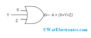
Three Input NOR
The 3-input NOR gate truth table and logical design is shown below:
| X | Y | Z | A |
| 0 | 0 | 0 | 1 |
| 0 | 0 | 1 | 0 |
| 0 | 1 | 0 | 0 |
| 0 | 1 | 1 | 0 |
| 1 | 0 | 0 | 0 |
| 1 | 0 | 1 | 0 |
| 1 | 1 | 0 | 0 |
| 1 | 1 | 1 | 0 |
Multi-Input NOR
Similar to multi-input OR and AND gates, an n-input NOR-gate can also be formed. When the number of inputs is odd, the unused input signal is kept LOW by connecting this unused signal to the power supply through pull-up resistors.
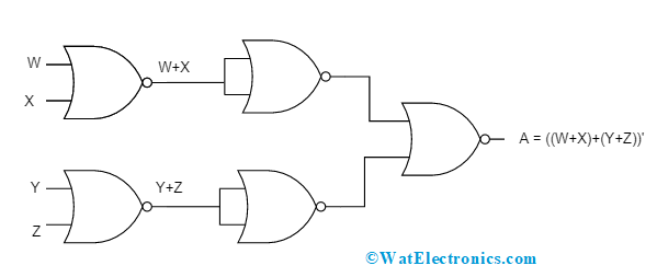
Multi Input NOR
Below is the logical expression and NOR gate design for 4-input NOR.
| W | X | Y | Z | A |
| 0 | 0 | 0 | 0 | 1 |
| 0 | 0 | 0 | 1 | 0 |
| 0 | 0 | 1 | 0 | 0 |
| 0 | 0 | 1 | 1 | 0 |
| 0 | 1 | 0 | 0 | 0 |
| 0 | 1 | 0 | 1 | 0 |
| 0 | 1 | 1 | 0 | 0 |
| 0 | 1 | 1 | 1 | 0 |
| 1 | 0 | 0 | 0 | 0 |
| 1 | 0 | 0 | 1 | 0 |
| 1 | 0 | 1 | 0 | 0 |
| 1 | 0 | 1 | 1 | 0 |
| 1 | 1 | 0 | 0 | 0 |
| 1 | 1 | 0 | 1 | 0 |
| 1 | 1 | 1 | 0 | 0 |
| 1 | 1 | 1 | 1 | 0 |
Deriving Basic Gates Using Negated OR Gate
As it is already discussed NOR is a universal gate. This makes it more flexible that, any basic logic gate can be derived using a NOT OR gate. The below section explains on NOR gate using basic gates.
AND using Negated OR
When the inputs are considered as X and Y, then for an AND gate, the desired output is X.Y. So, the below Boolean expression shows the derivation of NOR gate using and gates.
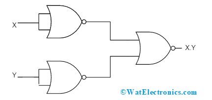
AND Using NOT OR Gate
Using Involution principle,
- Y = (X.Y)’
=> [(X+X)’ (Y+Y)’]’ = Idempotency principle
=> X.Y
OR using Negated OR
When the inputs are considered as X and Y, then for an OR gate, the desired output is X + Y. So, this Boolean expression is derived using NOR logic gate.
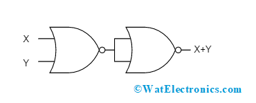
OR Using NOT OR Gate
Using Involution principle,
X + Y = ((X.Y)’ )’
- [(X + Y)]’
- X+Y -> Involution principle
NOT using Negated OR
When the input is considered as X, then for a NOT gate, the desired output is X’. So, this Boolean expression is derived using NOR logic gate.
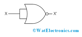
NOT Using NOT OR Gate
Using the Idempotency principle,
(X+X)’ = (X)’
Transistor Implementation of Negated OR
To design a NOR-gate using transistor, mostly two bipolar junction transistors are needed. Here, NOR logic gate is constructed using two NPN transistors, 10k Ohms resistors 2, 4-5k Ohm resistor 1, push buttons – 2, wires to establish connections between the components, LED display, and power supply. Below is the NOR gate circuit diagram that explains the functionality.
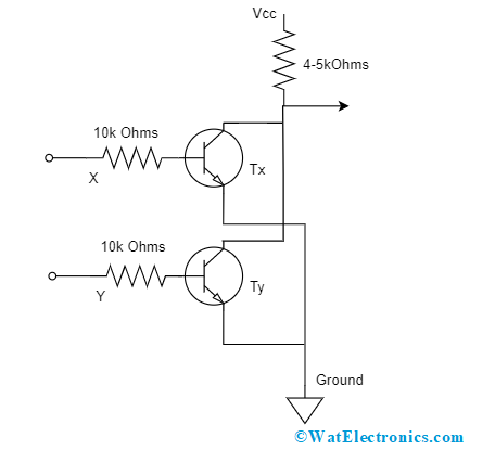
NOR Using Transistor
As per the above diagram, the two NPN transistors Tx and Ty are in parallel connection and the output pin has a connection with the collector ends of both the transistors. Both the inputs X and Y are connected to the base terminals of both the transistors correspondingly.
Now, based on the value and combination of inputs applied at the base terminals, the output changes respectively which is as per the NOT OR gate truth table.
To know the exact functionality of the NOR logic gate using a transistor, we need to analyze all four combinations of inputs.
Case 1: When X = 0 and Y = 0
When both the X and Y inputs are at a logic LOW state, then there exists no connection between the emitter and collector end of Tx and Ty. Because of this, the power supply reaches the collector ends of Tx and Ty. As the collector terminals of Tx and Ty are connected with LED display, the power supply reaches to output that corresponds to logic HIGH resulting in LED light glowing.
Case 2 : When X = 0 and Y = 1
In this condition, the input for the Tx transistor is 0 and the input for the Ty transistor is 1. When there is the power supply to the circuit, it passes to the collector ends of both Tx and Ty, then the current will pass only to the Ty that has Y input. As the input for X is ‘0’, there will be no connection in between the collector and emitter ends for the transistor Tx whereas there will be a direct connection between emitter and collector ends for Ty.
From here, the current reaches the entire circuit, but the emitter end has a connection with the ground which makes a ‘0’ potential difference between the ground and output terminal. Due to this, LED moves into OFF condition thus making the output as logic LOW.
Case 3: When X = 1 and Y = 0
When the X input is at logic HIGH and Y input is at logic LOW, the switch for Tx moves to OFF, and Ty becomes ON. This makes the output as logic LOW which is similar to case 2.
Case 4 : When X = 1 and Y = 1
Here, the inputs X and Y are at logic HIGH this means the power supply directly reaches to collector end through the 4k Ohm resistor. As both the inputs are at a HIGH state, this establishes a direct connection between the collector end of Tx and the emitter end of Ty. Whereas Ty is connected to the ground, the potential variation in between the collector end of Tx and emitter end of Ty becomes ‘0’. As the collector also has a connection with output, the LED display gets 0V i.e. the output is LOW.
NOR Gate Using MUX
Multiplexers are combinational circuits having multiple data inputs and providing a single output. These are also termed as data n selectors, universal logic circuits, many to one device, and parallel to serial converters. Mux devices are generally implemented in circuits to enhance the amount of data that can be transferred across the network within the specified amount of bandwidth and time. The below picture shows how the NOR logic gate is designed using a mux.
Here, OUT = Y’ when S0 equals to ‘zero’ and OUT = ‘0’ when s0 is ‘one’. So, a 2-input multiplexer acts like NOR-gate when the SEL of the multiplexer is connected to S0, D0 to Y’ and D1 to ground.
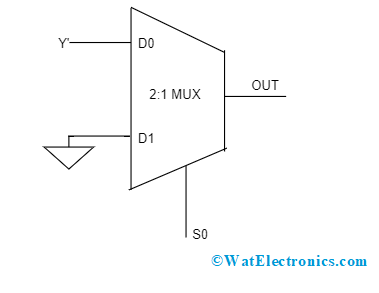
NOT OR Using Multiplexer
DTL Implementation of NOT OR Gate
The implementation of NOR using diode can be termed as Diode Transistor Logic (DTL) where the circuit uses a BJT transistor and general-purpose diodes. The logic behind the operation of this circuit is simple.
The collector and emitter end of the transistor are in parallel with the LED. When the transistor is in ON condition, the power supply bypasses all parts of the circuit through collector-emitter junctions which makes the LED move into an OFF state that is output is logic ‘0’.Below is the circuit diagram of DTL.
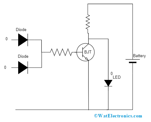
NOR Using Diode
The transistor moves into a conduction state only when either of the inputs is at logic ‘1’. Whereas when both the inputs are logic ‘LOW’, the transistor will stop conducting and so the entire power supply passes through the LED device thus making it ON which means that the output is logic ‘1’.
VHDL Code of Negated OR Logic Gate
This section explains the VHDL code implementation for a NOR logic gate:
library IEEE;
use IEEE.STD_LOGIC_1164.ALL;
use IEEE.STD_LOGIC_ARITH.ALL;
use IEEE.STD_LOGIC_UNSIGNED.ALL;
entity NOR Gate is
Port ( X : in std_logic;
Y : in std_logic;
A : out std_logic);
end NOR Gate;
architecture NOR1 of NOR Gate is
begin
A <= X NOR Y;
end NOR1;
NOT OR Gate IC
This is a two-input NOR logic gate IC that has 14 pins. The IC consists of 4 independent gates where each gate performs NOR logic gate functionality. These gates work on advanced silicon gate CMOS technology to gain higher functional speeds utilizing minimal power and every gate has buffered outputs. The outputs are directly interfaced to NMOS, TTL, and CMOS logic. This IC has an enhanced range of operating voltage and has wide functional conditions.
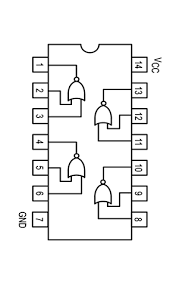
7402 IC
The functional characteristics of 7402 are:
Operating voltage ranges between 4.75 V to 5.25 V
- The LOW and HIGH levels of input voltages are 0.8 V and 2 V
- The HIGH and LOW levels of output currents are -0.4 mAmps and 16 mAmps
The electrical characteristics are:
- The HIGH and LOW-level input currents are 40 µAmps and -1.6 µAmps
- The HIGH and LOW level output voltages are 2.4 V and 0.4 V
The switching characteristics of 7404 are:
- The output propagation delay time at the level of LOW to HIGH has a maximum of 10 ns at a CL of 15 pF
- The output propagation delay time at the level of HIGH to LOW has a maximum of 15 ns at a CL of 50 pF
Advantages and Disadvantages
The advantages and disadvantages of NOR gate are as follows:
Advantages:
- NOR logic gates are cost-effective devices
- These devices require minimal space, less material for construction, and minimal complication too.
NOT OR Gate Applications
A few of the NOR Gate applications are explained as below:
- These are used in combinational circuits such as multipliers, multiplexers, half and full adders, and in ripple-carry adders.
- Also used in sequential circuits and in shift registers also
Please refer to this link to know more about XNOR Gate MCQs, NOR Gate MCQs
Please refer to this link to know more about OR Gate Advancements.
This is all about an overview of NOR logic gate. This article has given detailed exposure to the NOR logic gate truth table, circuit, design, applications, and advantages. Also, know how CMOS logic NOR are constructed and what are their performance characteristics?