NPN transistor is a type of bipolar junction transistor and it is the combination of two n-type and one p-type semiconductor. In this transistor, the p-type semiconductor is fixed in between both n-type semiconductors. Hence the two n-types are present in it. The majority of charge carriers of this transistor are electrons. This transistor includes three terminals namely emitter, base, and collector. The flow of the majority carriers in this type is from the emitter to the respective collector. This flow is responsible for the generation of current in the NPN transistor. This article discusses an overview of NPN transistor and its working.
What is a NPN Transistor?
A bipolar junction transistor is formed because of the connection established between two n-types and one p-type in the middle of it. So this is known as the NPN transistor. In this way, we can define the N-P-N transistor. For the applications of switching and regarding the amplification of the signals, this N-P-N transistor is preferred.

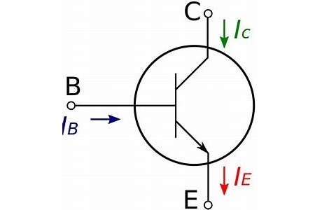
Symbol of NPN Transistor
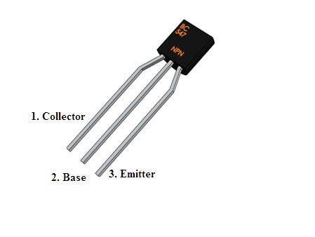
NPN Transistor Pin Out
The BC-547 transistor is a basic bipolar junction transistor N-P-N transistor that consists of a collector, base, and emitter as its terminals. At the collector pin, the current flows through the transistor. The base pin is responsible for controlling the applied bias to the transistor. The current gets drained out through the transistor.

NPN Transistor Pin Out
Construction
The N-P-N transistor is constructed by two diodes connected in such a way that its backs get connected to one another. These diodes connection made in such a way that the three terminals are formed known as collector base and emitter. The two junctions are formed in it one is emitter-base and the other is collector base.
The emitter-base junction is involved at the input side whereas the collector base is involved at the output side. The middle part of this transistor that is p-type is lightly doped this is the most important fact that is considered during its working. The emitter is considered to be doped moderately and the collector part is doped heavily.
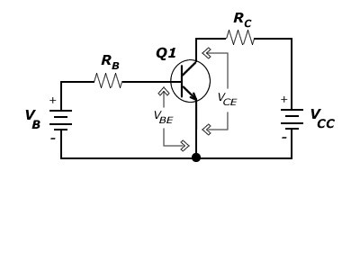
NPN Transistor Circuit
In the N-P-N circuitry, the emitter and the base junction are connected in the forward bias mode whereas the collector and the base junction are connected in the reverse bias mode. The collector of this transistor must be connected to the positive supply provided and the emitter is connected to the negative supply. The base is responsible for the controlling of ON and OFF switching states of the transistor.

N-P-N Transistor Circuit
NPN Transistor Working
The working of this transistor can be considered to be complex. As per the circuit diagram the connections are made. The junctions as mentioned the collector and the base junction in reverse bias and the emitter and the base junction in the forward bias.
There is a comparison is made between the forward and the reverse bias voltages as per that the forward voltage is small in comparison with the reverse-biased voltage.
As the forward biasing appears at the emitter terminal the movement in the majority of the carriers can be noticed towards the base. hence the current generated is referred to as emitter current. As the electrons entered into it the combination of holes with the electrons takes place in the p-type semiconductor.
As the base in this transistor is doped lightly only a few numbers of the electrons get recombined. Then the remaining electrons are responsible for the generation of the current referred to as base currency. This current finally enters into the collector region. As the junction of the collector and the base is reverse biased because of the highly attractive forces implied on it the electrons get collected in the terminal called the collector.
Finally, we can conclude that the emitter current generated is the sum of the collector and the respective base current.
NPN Transistor as a Switch
The complete switching operation is based on the amount of voltage applied to the terminal base. As the applied voltage exceeds the cut-off value the transistor can be seen in an operating mode called saturation region. The other condition is at which there is no voltage applied to the base.
This type of condition leads to the operating region referred to as a mode called cut-off. This type of operation is referred to as a switch. The type of switching involved in it is of lower cost compared to that of the relays that are conventional. In this switching phenomenon, the load that can be connected is a resistor or any other device can be connected to the switching output.
One of the practical and easier examples of the switch can be a led. During cut-off mode, the LED is in OFF mode. As the transistor is in the saturation region the device gets turned ON.
N-P-N Transistor Applications
The applications of NPN transistors include the following.
- The applications like switching mainly make use of the N-P-N transistor.
- The amplifier circuits include an N-P-N transistor.
- The Darlington transistors include N-P-N transistors during the applications of weak signals.
- The requirement of sinking the current paves the way for the utilization of the N-P-N transistors.
- The push-pull amplification circuitry includes the N-P-N transistors.
- The temperature measuring sensors utilize the N-P-N transistors.
- The log value converters include N-P-N transistors.
- For high-end frequency applications, this type of transistors is used.
Please refer to this for How to Select a Transistor.
In this way, an N-P-N transistor is designed. It is preferred during various applications. The presence of the majority of n-types made in it the majority of the carriers as electrons. The regions are doped lightly at the center responsible for the generation of base current.
The amount of bias is dependent upon or it is controlled from the base terminal the collector must get positive supply these are some of the operating restrictions of the N-P-N transistor.
After discussing this in detail and dealing with its various applications what is the type of bipolar junction transistor that can be preferred for amplification of the signals P-N-P or N-P-N?