The junction field effect transistor or JFET is a fundamental component in electronics that operates on the electric field control principle. It includes three terminals; gate (G), drain (D), and source (S). JFET is a voltage-controlled device compared to the Bipolar Junction Transistor (BJT). The current flow in JFET is because of the majority of charge carriers but the current flow in BJT is because of both majority and minority charge carriers. This article provides an overview of J310 JFET, its pinout, specifications, and applications.
What is J310 JFET?
The J310 transistor is an N-channel depletion JFET (junction gate field effect transistor) designed mainly for use in UHF and VHF amplifiers, mixers, amplifiers, and high-frequency oscillators. This is a high-Idss device, so its Idss is much higher than that of general JFETs such as 2N3819, MPF102, 2N4416, and many more. As a common gate amplifier, 12 dB at 450 MHz and 16 dB at 100 MHz can be realized.
JFET is made with a long semiconductor material channel that is doped to have either p-type (positive charge carriers) or n-type (negative carriers). So these transistors are voltage-controlled devices that are turned ON normally which means maximum current supplies throughout the source & drain whenever no voltage is provided to the gate terminal. So, the flow of current within a JFET is because of the majority of charge carriers which makes it a unidirectional device.
J310 JFET Pin Configuration:
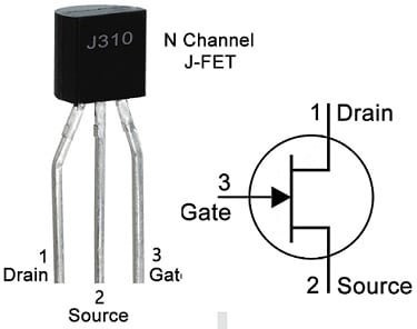
J310 JFET pin configuration is shown below. This transistor includes three terminals which are discussed below.

J310 JFET Pin Configuration
- Pin-1 (Drain): This terminal allows the flow of current into the chip.
- Pin-2(Source): This terminal controls the biasing of JFET.
- Pin-3 (Gate): The gate terminal connects to the ground which is an output of current supply from the chip.
Features & Specifications:
The features and specifications of J310 JFET include the following.
- This JFET has a high gain ability so that it amplifies or increases a signal from low level to above.
- It can also possess less noise ability, so once you try to change a small signal, then noise can be amplified thus utilizing a low noise and high gain transistor not only changes the signal but also decreases the noise significantly with that signal.
- This transistor can also have very low distortion which can also help in getting the original signal.
- The high sensitivity of this transistor makes it amplify extremely small or low-level signals to a higher level.
- This transistor can also have high amplification quality which means the quality of the output signal will be extremely good from each aspect.
- It has upto 100dB or above dynamic range, high-speed switching, and wideband gain.
- This transistor is available in the TO-92 Package.
- It is a N Channel depletion transistor.
- Its maximum gate-to-drain voltage must be -25V.
- The gate to source voltage maximum must be -25V
- Its maximum gate current is around 10mAmps.
- Gate to source cutoff voltage ranges from -2.0 to -6.5 volts.
- Its drain power dissipation maximum is 360mW.
- The typical low noise figure is Upto 2.7dB.
- Its maximum operating and storage temperature must be -55 to +150 Centigrade.
Equivalent & Alternatives
Equivalent J310 JFETs are; J309, J308, L310, J309, J111, U309, U310, BFW10, 2SK125-4, etc. Other JFETs are; MMBF4392LT1G, JFE150, MMBFJ177LT1G, MMBFJ175LT1G, MMBFJ111 JFET, etc.
How to Operate J310 JFET in a Circuit for a Long Time?
To operate J310 JFET safely, do not utilize this transistor to its total maximum ratings. Always stay below 20% of the complete maximum ratings. Maximum gate current must be 10mA so do not drive any load > 8mA. The maximum voltage from gate to source is 25V so do not drive any load > 20Volts. Always operate and store the transistor at >-55°C and < +150 °C temperature.
Crystal Oscillator Circuit with J310 JFET
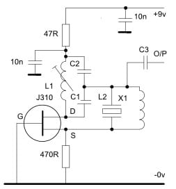
The crystal oscillator circuit with J310 JFET is shown below. This simple circuit uses low frequencies to a minimum of 120MHz with a series of resonant crystals on their overtone or fundamental mode. So the output can be received from the feedback tap which is shown below. Low impedance winding above L2 (or) from the J310 transistor’s drain terminal through a low-value capacitor is shown. The above stage must be utilized as a buffer to separate subsequent stages of the oscillator.

Crystal Oscillator Circuit with J310 JFET
Here, the combined series C1 & C2 resonate values with the L1 inductor at the preferred frequency & X1 crystal must have a basic (or) overtone series resonance as suitable at a similar frequency. Thus, C2 is five times above the C1 value.
Generally, an L2 inductor is required only at frequencies above 60MHz and should be selected to resonate through the whole parallel X1 capacitance at the oscillation frequency. If the above-shown circuit signs of free-running oscillation are controlled through L1 then L2 will be necessary. So, the X1 parallel capacitance will typically range from 4 pF – 6 pF at 60MHz frequencies.
Advantages & Disadvantages
The advantages of J310 JFET include the following.
- Advantages of Junction Field Effect Transistor (JFET)
- JFET provides good stability in different operating conditions.
- This transistor consumes less power which makes it very energy efficient.
- It has high input impedance which can be well suited mainly for amplifier circuits.
- These are fairly simple to utilize & do not need the complex biasing arrangements frequently found within other transistors.
- They don’t have gate current flow, thus simplifying circuit design within applications wherever current supply should be avoided.
The disadvantages of J310 JFET include the following.
- JFET is a unipolar device because the flow of current can be controlled throughout the charge carrier’s movement either holes or electrons.
- They can exhibit gate-to-source leakage currents, which is necessary within strict leakage current applications.
- Finding particular JFETs including specific characteristics can be difficult.
- It has less gain and thus cannot be utilized within high-gain applications.
- It is costly, which can affect the overall price of electronic devices.
Applications
The applications of J310 JFET include the following.
- J310 JFET is used in oscillators, mixers, VHF or UHF amplifiers, signal amplification, etc.
- This JFET is used in electronic circuits for high-frequency and signal amplification applications like switching and amplifiers.
- It is used in oscillator and RF amplifier circuits up to 500 MHz.
- These can be used in voltage amplifiers, electronically controlled switches, etc.
- These JFETs can be used as choppers, voltage-controlled resistors, phase shift oscillators, current limiters, etc.
- These are used within low-noise applications like; analog signal processing.
- It can be used as choppers and buffers.
- This JFET can be used within oscillatory circuits, cascade amplifiers, etc.
- It is used in high-frequency mixers or amplifiers, sample and hold, oscillators, and very low capacitance switches.
Please refer to this link for the J310 JFET Datasheet.
Thus, this is an overview of J310 JFET, pinout, features, specifications, circuit, working, advantages, disadvantages, and applications. This is an N-channel type JFE, available in TO92, and is designed mainly for amplifiers and high-frequency oscillators. Thus, its voltage is 25V, the current supply is 10 mA, and its frequency is up to 500 megahertz. This JFET can be used as a voltage amplifier, switch, phase shift oscillator, current limiter, and chopper. So here is a question for you, what is FET?