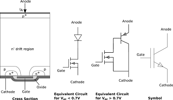
Insulated-Gate-Bipolar-Transistor
The term IGBT is a short form of insulated gate bipolar transistor, it is a three-terminal semiconductor device with huge bipolar current-carrying capability. Many designers think that IGBT has a CMOS i/p and bipolar o/p characteristic voltage controlled bipolar device. So, this device is designed to make use of the benefits of both BJT and MOSFET devices in the form of monolithic. It combines the best qualities of both to attain the characteristics of an optimal device.
This device is apt for several applications such as used in power electronics, particularly in PWM(Pulse Width Modulated), UPS (Un interruptible Power Supplies), SMPS (Switched-Mode Power Supplies), and other power circuits. It increases the efficiency, dynamic performance and reduces the level of the audible noise. It is similarly fitted in the of resonant mode converter circuits. Optimized IGBT is accessible for both low switching loss and low conduction loss.
What is an IGBT?
The IGBT (insulated gate bipolar transistor) is a three-terminal electronic component, and these terminals are termed as emitter, collector and gate. Two of its terminals namely collector and emitter are associated with a conductance path and the remaining terminal ‘G’ is associated with its control. The sum of amplification is achieved by the IGBT is a ratio between its input and output signal. For a conventional BJT, the amount of gain is almost equal to the ratio of the o/p current to the i/p current that is called a beta.
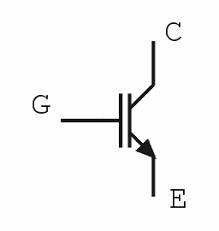
IGBT Symbol
For a MOSFET (metal oxide semiconductor field effect transistor), there is no i/p current as the gate terminal is isolated from the main current-carrying channel. Thus, the gain of the field effect transistor equals to the an FET’s gain is equal to the ratio of o/p current change to i/p v change, Then the IGBT can be treated as a power BJT and the base current of this transistor is provided by an MOSFET.The IGBT is mainly used in small-signal amplifier circuits like BJT or MOSFET When the transistor combines the lower conduction loss of a BJT and MOSFET, then an ideal solid state switch occurs which is perfect for in various applications of power electronics.
An IGBT is simply switched “ON” and “OFF” by triggering and disabling its Gate terminal. A constant +Ve voltage i/p signal across the ‘G’ and the ‘E’ will retain the device in its “ON” state, while deduction of the i/p signal will cause it to turn “OFF” like BJT or MOSFET.
Basic Structure of IGBT
The basic structure of the N-channel IGBT is shown below. This structure is plain that the IGBTs silicon cross section is almost equal to that of a vertical power MOSFET except P+ injecting layer. It shares the same structure of MOS gate & P-wells with N+ source regions. In the following structure, the N+ layer is located at the top is called as the source and the bottom layer is called as a drain or collector.
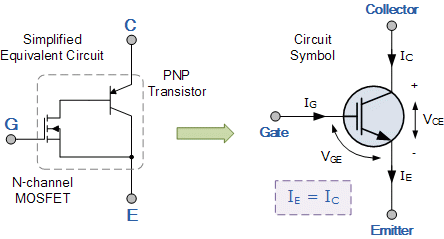
Basic Structure of N-Channel IGBT
IGBT takes a parasitic thyristor includes the 4-layer NPN structures. There are some IGBs that are fabricated without the N+ buffer layer is called as NPT IGBTS non punch through), whereas some IGBTs are fabricated with the N+ buffer layer called as PT IGBTs (punch through). The performance of the device can considerably increase by existing the buffer layer. The operation of an IGBT is faster to that of power BJT than a power MOSFET.
Circuit Diagram of an IGBT
Based on the basic structure of the IGBT, a simple circuit can be drawn using PNP and NPN Transistors, JFET, OSFET, that is shown in the below figure. The collector terminal of the NPN transistor is connected to the base terminal of the PNP via JFET transistor. These transistors signify the parasitic thyristor which creates a regenerative feedback loop. The RB resistor signifies the shorting of the base-emitter terminals of the NPN transistor to ensure that the thyristor doesn’t latch up, that will lead to the IGBT latch-up.
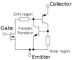
Circuit Diagram of an IGBT
The JFET transistor signifies the construction of current b/n any two adjacent IGBT cells. It allows the MOSFET and supports most of the voltage. A circuit symbol for the IGBT is shown below, that consists of three terminals namely emitter, gate and collector.Switching Behavior of IGBT
Switching Behavior of IGBT
These devices are mostly used as switches, for instance frequency converter and chopper applications, the variation of a diode is most important, because when the switching of the IGBT is OFF, then the current is determined by the load, that is inductive in many cases.
By connecting appropriate diodes, the current flow is allowed. When this transistor is switched on again, the current flowing in a diode at first works like a short. The voltage can be blocked by removing the stored voltage. This looks as a surplus current added to the load current which is called as the reverse recovery current of the diode ‘Irr’. The max of Irr occurs (di/dt = 0) when the amount of the sudden voltages through the IGBT & the diode matches the supply voltage. When the IGBT is turned ON, then the current changes which make an over-voltage point by the change in the current in the dependent inductances agreeing to ∆VCE = Lσ × di/d
NPT-IGBT and PT-IGBT
The NPT and PT-IGBT’s are developed by IXYS Corporation. The physical construction of the NPT and PT IGBTs are shown below. The structure of PT consists of an extra buffer layer that executes two functions they are, 1) The failure can be avoided by punch through action as the depletion area expansion at applied high voltage is controlled by this layer. 2).Fail current can be reduced when it turns off & reduces the fall time of the IGBT because the holes are inserted by the collector of the P+ incompletely recombine in this layer.
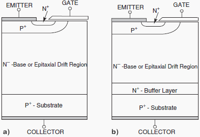
NPT-IGBT and PT-IGBT
The basics of NPT-IGBT, IXYS Corporation 4 IXAN0063 and Abdus Sattar have equal breakdown voltage and these are applicable for AC applications. The PT-IGBTs have less breakdown voltage and these are relevant for DC circuits where these devices are not essential to support voltage in the reverse direction.
Difference between NPT-IGBT and PT-IGBT
It is a voltage controlled device and it needs a small amount of voltage on the gate terminal to keep conduction through the device.
This is a unidirectional device because, it can only change current in the forward direction that is collector-to-emitter.
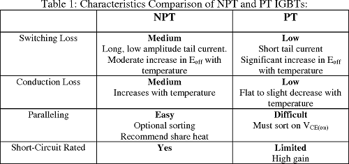
Difference between NPT-IGBT and PT-IGBT
The principle of the BJTs is very similar to the N-channel MOSFET. The main difference is, the current existing by the conducting channel when current supplies through the device in its ON state is very small in the IGBT, due to this reason, the ratings of the currents are high when matched with an MOSFET.
Advantages and Disadvantages of IGBT
The main advantages of IGBT compared with various kinds of transistors are low ON resistance, high voltage -capacity, fast switching speed, ease of drive and joined with zero gate drive current creates a good option for sensible speed, and various high voltage applications like PWM, SMPS, variable speed control, AC to DC converter powered by solar and frequency converter applications which operates with a hundred’s of KHz.
The main disadvantages are: The speed of the Switching is lower to a Power MOSFET and higher to a BJT. The collector current following due to the minority charge carriers roots the turnoff speed to be slow. 2. There is a chance of latch up due to the internal structure of PNPN thyristor.
Thus, this is all about IGBT working and IGBT applications. We have observed that the IGBT is a semiconductor switching device that has an o/p characteristic of a BJT, but it is controlled like an MOSFET. We believe that you have got a better understanding of this concept. Furthermore, any doubts regarding the IGBT applications or electrical and electronic projects, please give your feedback by commenting in the comment section below. Here is a question for you, what are the differences between BJT, MOSFET and IGBT?
Photo Credits
- Circuit Diagram of an IGBT by wikimedia
- NPT-IGBT and PT-IGBT by electrical-engineering-portal