The most popular semiconductor technology (MOSFET technology) obtainable today is the CMOS technology. The term CMOS stands for complementary MOS technology. This is the most important semiconductor technology for ASICs, microprocessors, memories, etc. The main benefit of CMOS technology over NMOS and Bipolar technology is the power dissipation – when the circuit activates then only the power dissipates. This allows fitting several CMOS gates on an IC (integrated circuit) than in Bipolar & NMOS technology. This article discusses the CMOS and NMOS technology differences and their advantages.
What is IC Technology?
The Si-IC technology can be categorized into three types namely: Bipolar, MOS (Metal oxide semiconductor), and BiCMOS.
The construction of the bipolar transistors has PNP or NPN structures. In these kinds of transistors, the tiny amount of current in the solid base layer controls huge currents between the terminals of an emitter and collector. Base currents limit the additional density of the bipolar devices.
IC Technology
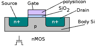
Metal oxide semiconductor (MOS) is further divided into different technologies beneath NMOS, PMOS, and CMOS. These technologies comprise a semiconductor, a metal gate, and oxide. At present, Polysilicon is generally used as a gate terminal. When the voltage is applied to the gate terminal, then it controls the flow of current between the terminals of the source and drain. Since they use less power, and metal oxide semiconductor permits higher integration.
BiCMOS Technology can be built with the CMOS and Bipolar transistors; these are incorporated on a similar semiconductor chip. CMOS technology gives high input and low output impedance, symmetrical noise margins, high packing density, and low power dissipation. BiCMOS technology has finished it possible to unite bipolar devices and CMOS transistors in a single process at a sensible cost to get the high-density integration of MOS logic
CMOS and NMOS technology Difference
The CMOS and NMOS technology differences can be simply distinguished with their working principles, advantages, and disadvantages as discussed.
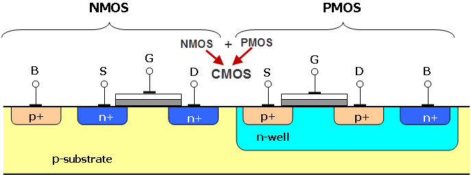
Differences between CMOS and NMOS Technology
CMOS Technology
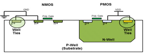
CMOS technology is used in digital logic circuits to construct ICs, microprocessors, static RAM, microcontrollers. This technology is also used in numerous analog circuits like image sensors, data converters, and in highly integrated transceivers. The main features of this technology are high noise immunity and low static power consumption.
CMOS Technology
When the pair of transistors is in OFF condition, the grouping of series draws important power only throughout switching between ON & OFF states. So, MOS devices do not generate as much dissipate heat as other types of logic. For instance, TTL or MOS logic have normally some standing current even when not the varying state. This permits a high density of logic tasks on a chip. Due to this cause, CMOS technology is most widely used and is executed in VLSI chips.
Advantages of CMOS Technology
CMOS technology devices are used in a variety of applications with analog circuits such as data converters, image sensors, etc. The benefits of CMOS technology over NMOS technology include the following.
- Static power consumption is very slow.
- The complexity of the circuit reduces
- The high density of logic functions on a chip
- Static power consumption is very low
- High noise immunity
CMOS Inverter
For any IC technology, the logic inverter plays a vital role in the designing of a digital circuit, Once the process of an inverter circuit is cautiously understood, the consequences can be extended to the logic gates design and complex circuits.
CMOS-Inverter
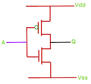
CMOS inverters are MOSFET inverters, which are most widely used in chip design. These inverters can function at high-speed and with less power loss. Also, this inverter has good logic buffer characteristics. The small explanation of the inverters gives a basic understanding of the operation of the inverter. MOSFET states at different input voltages, and power failures due to electrical current.
A CMOS inverter has two transistors namely a PMOS transistor and an NMOS transistor that is connected to the gate and drain terminals, a VDD (voltage supply) at the PMOS source terminal, and a GND terminal connected to the NMOS source terminal, where the input voltage is connected to the gate terminals and output terminal is connected to the drain terminals. It is significant to observe that the CMOS doesn’t have any resistors, which creates more power capacity than a regular resistor MOSFET inverter.
As the voltage at the CMOS device input changes between 0 & 5 volts, the condition of the NMOS and PMOS changes accordingly. If we mold each transistor as an easy switch triggered by the input voltage, the inverter’s actions can be seen very simply.
NMOS Technology
The acronym of NMOS is a negative channel metal oxide semiconductor; it is pronounced as en-moss. It is a kind of semiconductor that charges negatively. So that transistors are switched by the movement of the electron. Indifference, Positive channel MOS -PMOS works by moving electron positions. NMOS technology is faster than PMOS.
NMOS Technology
NMOS Inverter
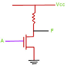
Inverter circuit o/ps a voltage representing the opposite logic-level to its i/p. The NMOS inverter diagram is shown below which constructed using a single NMOS transistor is coupled with a transistor.
NMOS-Inverter
Why CMOS Technology is Preferred Over NMOS Technology
CMOS stands for Complementary Metal-Oxide-Semiconductor whereas NMOS is a negative channel metal oxide semiconductor. CMOS and NMOS are two logic families, where CMOS uses both MOS transistors and PMOS for design and NMOS use only field-effect transistors for design.
CMOS is selected over NMOS for the designing of an embedded system. CMOS transmits both logic 0 logic 1 and NMOS only logic 1 i.e, VDD. The output after crossing through one, the NMOS gate would be VDD-Vt. So, CMOS technology is preferred.
In CMOS logic gates, a collection of n-type MOSFETs is located in a pull-down network between the low voltage power supply rail and the o/p. In its place of the load resistor of NMOS logic gates, CMOS has a set of P-type MOSFETs in a pull-up n/w between the high voltage rail and the o/p. Thus, if both transistors have their gates connected to a similar input, the p-type MOSFET will be ON when the n-type MOSFET is OFF, and vice-versa.
CMOS and NMOS both moved by the expansion in digital technologies, that are used to build the integrated circuits. Both are used in several digital logic circuits and functions, static RAM, and microprocessors. These are used in analog circuits as data converters and image sensors and also used in Trans-receptors for several modes of telephone communication. While both have a similar function as transistors for both analog and digital circuits, but a lot of people still select the CMOS technology to the final for its many advantages.
Please refer to this link to know more about Analog Circuits MCQs & VLSI MCQs
Please refer to this link for CMOS MCQs
As contrasted to the NMOS, the CMOS technology is top in excellence. Particularly, when it comes to its features like low-static power utilization & noise resistance, CMOS technology keeps energy and it does not generate heat. Though costly, a lot of people prefer the CMOS technology due to its difficult work of art that makes it tough for the black market to manufacture the technology used by the CMOS.
The CMOS and NMOS technology differences along with their inverters, differences are discussed in brief in this article. Thus, CMOS technology is top of the embedded system design. For a better understanding of this technology, please post your queries as your comments below.