Both p-n-p and the n-p-n transistors are the basic transistors which come under the category of bipolar junction transistors. These are used in the various amplifications circuits and the modulating circuits. The most frequent one among its applications is it’s fully ON and the OFF operating mode which is referred to as switch.
NPN and PNP transistors are bipolar junction transistors, and it is a basic electrical and electronic component which is used to build many electrical and electronic projects. The operation of these transistors involves both electrons and holes. The PNP and NPN transistors allow current amplification. These transistors are used as switches, amplifiers or oscillators. Bipolar junction transistors can be found either as large numbers as parts of integrated circuits or in discrete components. In PNP transistors, majority charge carriers are holes, whereas in NPN transistors, electrons are the majority charge carriers. But, field effect transistors have only one type of charge carrier.
The formation of these transistors is based on the diodes with the junction p-n. As in the n-p-n transistors n-types are in majority therefore there includes excess amount of electrons as the charge carriers. In p-n-p transistors there are two p-types in it resulting in the majority charge carriers as holes.
The main difference between the NPN and PNP transistor is, an NPN transistor turns on when the current flows through the base of the transistor. In this type of transistor, the current flows from the collector (C) to the emitter (E). A PNP transistor turns ON, when there is no current at the base of the transistor. In this transistor, the current flows from the emitter (E) to the collector (C).Thus, knowing this, a PNP transistor turns ON by a low signal (ground), where NPN transistor turns ON by a high signal (current).
Difference between NPN and PNP Transistors and their Making
PNP Transistor
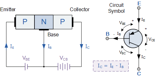
The PNP transistor is a bipolar junction transistor; In a PNP transistor, the first letter P indicates the polarity of the voltage required for the emitter; the second letter N indicates the polarity of the base. The working of PNP transistor is the exact opposite to the NPN transistor. In this type of transistor, the majority charge carriers are holes. Basically, this transistor works the same as the NPN transistor. The materials which are used to construct the emitter, base and collector terminals in the PNP transistor are different from those used in the NPN transistor. The PNP transistor bias setup is shown in the below figure. The base-collector terminals of the PNP transistor are always reversed biased, then the negative voltage must be used for the collector. Therefore, the base terminal of the PNP transistor must be negative with respect to the emitter terminal, and the collector must be negative than the base.
Making of PNP Transistor
The PNP transistor configuration is shown below. The characteristics of both PNP and NPN transistors are similar except that the biasing of the voltage and current directions are reversed for any one of the possible three configurations such as a common base(CB), common emitter(CE) and common collector(CC).The voltage between the base and emitter terminal VBE is negative at the base terminal and positive at the emitter terminal because for a PNP transistor, the base terminal always biased negative with respect to the emitter. Also, the emitter voltage is positive with respect to the collector (VCE).
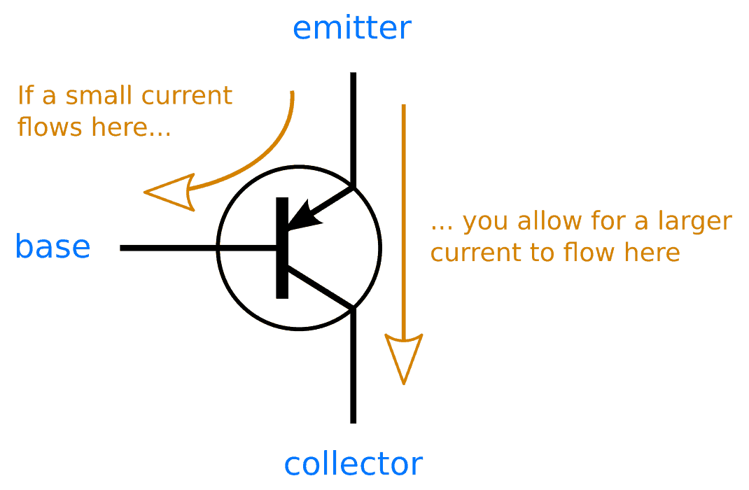
The voltage sources are connected to a PNP transistor, which is shown in the figure. The emitter is connected to the Vcc with the RL, this resistor limits the max current flowing through the device, which is connected to the collector terminal. The base voltage VB is connected to the base resistor RB, which is biased negative with respect to the emitter. To cause the base current to flow during a PNP transistor, the base terminal must be more negative than the emitter terminal by approx. 0.7volts or a Si device.
The fundamental difference between a PNP and a PN transistor is the proper biasing of the transistor junctions; the current directions and the voltage polarities are always opposite to each other.
Basics of P-N-P
The p-n-p transistors are formed with n-type present in between the p-types. The majority of the carriers those are responsible for the generation of the current are in this transistor are holes. The working operation is similar to that of n-p-n. But the applications of the voltages or currents in terms of polarity are different.
NPN Transistor
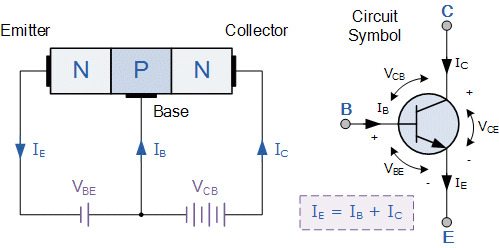
The NPN transistor is a bipolar junction transistor, In an NPN transistor, the first letter N indicates a negatively charged layer of material and a P indicates a positively charged layer. These transistors have a positive layer, which is located in-between two negative layers. NPN transistors are generally used in circuits for switching, amplifying the electrical signals that pass through them. These transistors comprise three terminals namely, base, collector and emitter and these terminals connect the transistor to the circuit board. When the current flows through the NPN transistor, the transistor base terminal receives the electrical signal, the collector makes a stronger electric current than the one passing through the base, and the emitter passes this stronger current on to the rest of the circuit. In this transistor, the current flows through the collector terminal to the emitter.
Generally, this transistor is used because it is so easy to produce. For an NPN transistor to work properly, it needs to be formed from a semiconductor material, which carries some electric current, but not the maximum amount as very conductive materials like metal. “Si” is one of the most commonly used semiconductor, and NPN transistors are the easiest transistors to make out of silicon. The application of an NPN transistor is on a computer circuit board. Computers need all their information to be translated into binary code, and this process is accomplished through a plethora of small switches flipping on and off on the computers circuit boards. NPN transistors can be used for these switches. A powerful electric signal turns the switch on, whereas a lack of a signal turns the switch off.
Making of NPN Transistor
The construction of an NPN transistor is shown below. The voltage at the base terminal is positive and negative at the emitter terminal because of an NPN transistor. The base terminal is always positive with respect to the emitter terminal, and also collector supply voltage is positive with respect to the emitter terminal. In NPN transistor, the collector is connected to the VCC through the load resistor RL. This load resistor limits the current flowing through the maximum base current. In this transistor, the movement of electrons through the base terminal that constitutes transistor action. The main feature of the transistor action is the link between the input and output circuits. Because, the transistor amplifying properties come from the consequent control that the base employs upon the collector to emitter current.
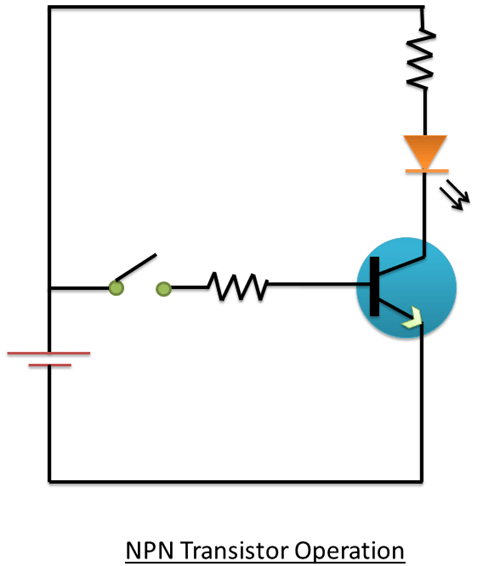
The transistor is a current operated device. When the transistor is switched on, the large current IC flows between the collector and emitter within the transistor. However, this only happens when a small biasing current Ib flows through the base terminal of the transistor. It is a bipolar NPN transistor; the current is the ratio of these two currents (Ic/Ib), called the DC current gain of the device and it is denoted with the symbol “hfe” or nowadays beta. The value of beta can be large up to 200 for standard transistors, and it is this ratio between Ic and Ib, which makes the transistor a useful amplifier. When this transistor is used in an active region, then Ib provides the input and Ic provides the output. Beta has no units as it is a ratio.
The current gain of the transistor from the collector to the emitter is called alpha that is, Ic/Ie, and it is a function of the transistor itself. As the emitter current Ie is the sum of a small base current and large collector current, the value of the alpha is very close to unity, and for a typical low power signal transistor this value ranges from about 0.950 to 0.999.
Difference Between NPN and PNP Transistor:
Bipolar Junction transistors are three terminal device and these are made of doped materials, often used in amplifying and switching applications. In essence, there are a couple of PN junction diodes in every BJT. When the pair of diodes joined then it forms a sandwich that places a type of semiconductor in between the same two types. Therefore, there are only two types of bipolar sandwich, which are namely PNP and NPN. In semiconductors, the NPN’s has characteristically higher electron mobility compared to the hole mobility. Therefore, it permits a large amount of current and operates very fast. And also, the making of this transistor is easy from silicon.
- Both PNP and NPN transistors are composed of different materials and current flow of these transistors is also dissimilar.
- In an NPN transistor, the current flows from the collector (C) to the Emitter (E), whereas in a PNP transistor, the current flows from the emitter to the collector.
- PNP transistors are made up of two layers of P material with a sandwiched layer of N The NPN transistors are made up of two layers of N material and sandwiched with one layer of P material.
- In an NPN transistor, a positive voltage is given to the collector terminal to produce a current flow from the collector to For PNP transistor, a positive voltage is given to the emitter terminal to produce current flow from the emitter to collector.
- The working principle of an NPN transistor is such that when you increase current to the base terminal, then the transistor turns ON and it conducts fully from the collector to emitter. When you decrease the current to the base terminal, the transistor turns ON less and until the current is so low, the transistor no longer conducts across the collector to emitter, and shuts OFF.
- The working principle of a PNP transistor is such that when the current exists at the base terminal of the transistor, then the transistor shuts OFF. When there is not current at the base terminal of the PNP transistor, then the transistor turns ON.
This is all about difference between NPN and PNP transistors which are used to build many electrical and electronic projects. Furthermore, any queries regarding this topic or electrical and electronics projects you can give your feedback by commenting in the comment section below.
Comparison in between N-P-N and P-N-P Transistor
1). In this the majority of n-types are present.
1). In this the majority of p-type materials are present.
2). The majority of the concentrations of the carriers are electrons.
2). The majority of the concentrations of the carriers in this type of transistors are holes.
3). In this if the terminal base is supplied with the increased amounts of current then the transistor gets switch to ON mode.
3). In this case for the low values of the currents the transistor is ON. Otherwise for high values of currents transistors it is OFF.
4). The symbolic representation of n-p-n transistor is
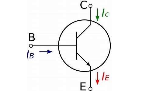
Symbol of N-P-N Transistor
4). The symbolic representation of p-n-p transistor is
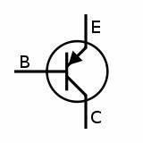
Symbol of P-N-P Transistor
5). In the n-p-n transistor the flow of current is evident from the collector to the emitter terminals.
5). In the p-n-p transistor the flow of current can be seen from the terminals of the emitter to the collector.
6). In this transistor the arrow is pointing out.
6). In this transistor the indication of arrow is always pointing in.
The arrows in the transistors both n-p-n and p-n-p shows the main differences between the transistors. The arrow in n-p-n is pointed towards the emitter whereas for p-n-p the arrow is in the reverse direction. In both the cases the arrow indicates the direction of the flow of current.
Hence the construction of n-p-n and the p-n-p is simple. The operating will be same but its polarities of biasing differ. Now after discussing regarding the basics of n-p-n and the p-n-p can you tell which one is preferred during amplification and why?
Please refer to this for How to Select a Transistor.
Please refer to this link to know more about Transistors MCQs.
Photo Credits:
- PNP Transistor by wikimedia
- Making of PNP Transistor by electronics-tutorials
