Semiconductors formed with differently doped p-type and n-type material on a single crystal forms the basic electronic devices like diodes, transistors, etc. These have their own significance in the development of modern electronic systems. Basics of electronics are dependent on the characteristics of such components. The characteristics of voltage and current help to analyze the equipment better. This article discusses what is a dc load line and its significance.
What is a DC Load Line?
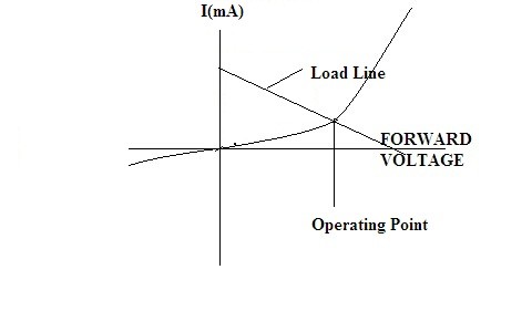
A circuit supplied with dc power as the external source of the circuit. There exist both alternating and direct currents in the circuit. The reactive components of the circuits are made zero and the straight line is drawn above the voltage-current characteristics curves. Hence these results in the formation of intersecting point referred to an operating point. The straight that is drawn for this purpose is defined as the DC load line.
Q Point in a DC Load Line
For any non-linear circuitry, if the analyses of its characteristics curve were done it is based on voltage and current parameters. During this graphical analysis as the characteristic curve is plotted above that straight line is drawn. This straight line is termed as dc load line because at this point reactive components are zero.
This is the constraint applied to the non-linear element by the external circuit. Hence the characteristic curve and the straight line are dawn above each other so that they can intersect each other at a point. The intersection point formed in between is known as Q point. It is also referred to as the correct DC operating point.
Significance
- The linear analysis of the circuit is obtained for the non-linear devices like diode or transistors by using this concept.
- The main intention behind the analysis of the load line is to find the operating point referred to as the quiescent point (Q-point).
- The Q-points formed by the dc load line are the centers at which the voltage and current parameters equivalent to each other for both the parts of the circuit.
- For transistor like BJT, in this case, the operating regions formed here because of the load line analysis method makes the device to remain in an active region.
- The signals that should be amplified are lesser than millivolts. The active region concept define by load analysis method is important here so that the amplification process is carried out here.
- From this, the operating point obtained is essential while drawing the ac load lines.
- If the resistance is constant and the dc voltage applied to the circuit varies. The load lone concept is significant for analyzing the circuit in an efficient manner.
DC Load Line of a Diode and Its Equation
DC load line for a non-linear device is drawn by making the reactive components as zero. Hence a diode is considered as a non-linear device and its voltage and current characteristics are exponentially related to each other. The formation of the intersection point for the characteristic curve and the straight line or dc-load line can be analyzed better by considering the example for the diode as in forward bias condition.
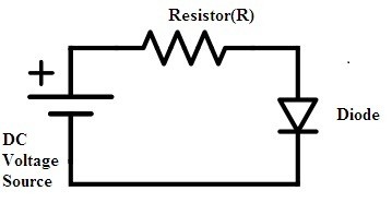
Let us consider a diode connected to the resistor(R), source of voltage (VDD) in series. The diode is connected in forward bias so that the forward current and the forward voltages flowing through the circuit. As per the Kirchhoff’s current law, the current flowing through the diode (ID) and the resistor (IR) is equal.
ID = IR
Analysis of the circuit is done by applying Kirchhoff’s voltage law (KVL). This law results in the formation of the final equation for the dc load line. Here the dc voltage is the biasing voltage of the circuit by keeping any further reactive components as zero.

diode-operating-in-forward-bias-for-the-analysis-of-dc-load
Once the Kirchhoff’s voltage law is applied to the circuit an equation is obtained for voltages and currents in the circuit.
VDD = VD + IDR
VD = IDR-VDD
Where VDD, is the applied dc source voltage and VD is the voltage across the diode. Hence the above can be considered as the equation for the diode. The voltage and current characteristics of the diode in forward bias condition can be drawn. By our previous analysis on the condition of the diode in forward bias applied a voltage and the generated current in the circuit are exponentially related to each other.
After a certain cut-off voltage, the diode starts operating in forward bias condition. To this slope, the technique is considered and a straight line on the v-i characteristics is drawn. The slope here for the above general circuit for the diode is VDD/R. Then the intersection of the lines results in the formation of diode operating point as already discussed.

dc-load-line-and-the-formation-of-operating-point
In this way, the analysis for the dc-load line is done for the non-linear device like a diode. Depending on the type of non-linear device some part of the analysis differs but the technique remains the same. This type of method comes under the graphical analysis because here the characteristics curve is considered for the formation of the dc-load line.
Once the characteristics curve is formed the slope is identified then with respect to that line is drawn. Everything is graphical here. In this way, the analysis for this is done in the above article. The main purpose of the analysis of the dc load line is that operating point is formed that is accurate in all terms and helpful for the further processing of the circuit. But for the overall analysis of the circuit Kirchhoff’s laws play a major role.
Please refer to this link to know more about Regulated DC Power Supply MCQ’s.
This is for the diode but transistor is also a non-linear device then based on its configurations the operating point is formed. Then what must be the reason so that to operate BJT the operating point mostly should remain in the active region and why the active region is preferred above the remaining other regions?