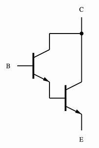
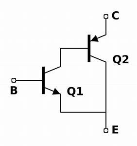
Darlington transistor is a pair of transistors that are connected in such a way that it enhances the features of the respective application. This transistor pair is invented by Sydney Darlington. It is formed in such a way that either two P-N-P or N-P-N transistors are connected so that the emitter of the one transistor is connected to the base of the other transistor. Both the transistors interlinked so that one can act as input other can refer to as output one.
The output of the transistor is given to the second transistor as input. So that it can be used in those fields where it is the higher necessity of amplification is required. These transistors provide the resultant value with the gain at it its highest. The input currents applied at the lower values but output gain is produced to be high.
What is Darlington Transistor?
The combination of the transistors either P-N-P or N-P-N of BJT type connected in order to form a pair is known as Darlington Transistor. This pair of transistors is efficient in terms of gain. The interconnection between the pair provides the current produced at the emitter terminal acts as the input current for the terminal base of the next transistor. Hence this pair is also referred to as “Super-Alpha Circuit”.
Working of Darlington Transistor
A Darlington transistor is a pair of transistor but these transistors are considered to be one while performing an operation. This works under the application of the low base currents and can operate the devices that of larger in terms of power values. The gain because of this transistor is considered to be high.
A bipolar junction transistor (BJT) can provide the current gain but when considered during amplifications it requires more amount of current gain. Hence the formation of the Darlington pair proven to be much useful in such cases. As the sufficient value of the current is supplied at the terminal base such that it plays a major role in the flow of the current from the collector. This indicates that BJT is entered in the saturation mode. This output is connected to the next transistor and further process continues.
The BJT is known for its characteristics of switching the devices ON and OFF. Whether it is P-N-P‘s configuration or the N-P-N’s configuration the follow up is same towards the applications.
Darlington Transistor Symbol
This symbol consists of pair of either N-P-N or P-N-P transistors interconnected.

Symbol of Darlington Transistor Pair Configuration of N-P-N
Basic Darlington Transistor Configuration
Let us consider two N-P-N transistors connected through their respective collectors. So that the emitter terminal in which the current is produced it’s been provided to the base of the second transistor. It acts as the input of the second transistor. Now the current at the terminal collector becomes the multiplication value of beta along with the base current. Hence the gain value of the current is maintained at the unity.
The final value of the current at the collector is the sum of the individual currents at the first transistor and the second transistor. But the current at the terminal base of the second transistor is equal to the emitter terminal current of the first transistor.
As both the transistors have their individual gains. These gains are multiplied together which gives the overall gain of the Darlington pair. Hence the product in between shows that the overall gain of the transistor is high. Similarly there will be a huge increase in the resistance value.
Applications
The applications of these transistors are
- It is highly capable of detecting the current value passed one it comes in to skin contact. Hence it provides a great application in the sensitive touch devices like touch pad etc…
- For the high current requirements these transistors are utilized.
- The motors or it can be relays where the control of these devices is provided based on the computer this pair of transistors proven to be helpful.
- These transistor pairs are used in amplification circuits where the gain required being high.
The above are the some of the applications of the Darlington pair of transistors.
Example
The pair of transistors N-P-N is connected and these are useful as a switch for a lamp. This lamp operates at 10V 50W. By neglecting the drops at the voltages the gain at the connected first transistor is to be 30. The current gain at the second transistor is at 60.then find the value of the current at the terminal base?
Sol: Now the current generated at the collector = the current required to switch on the lamp.
I Lamp= P/V
I Lamp=50/10= 5 Amps
Given the beta 1= 30, beta 2= 60
The equation used to find the current at the terminal base is
Therefore after substitution the current at the base is
I B= 5/ (30+ (30*60) +60)
I B= 2.6 m Amps
Hence from the above problem it can be concluded that for the small amount of the currents formed at the base a lamp with 50 watts can be made to switch ON and as well as OFF.
In case if the two transistors that are used is of some bipolar type configuration then the current gain value of both the transistors is considered to be equal.
Therefore the current at the terminal equation gets simplified and considered as
I C= I B
A Darlington transistor consists of minimum value of the voltage drop in between the terminals of the emitter and the base. The respective base terminal present in this pair is sensitive in a manner that any changes at the input it gets responded. But overall drop is the combination of the individual transistors.
The resultant value of the voltage drop is incremented in such a way that a heat sink must be provided for the purpose of cooling. This pair of Darlington is sensitive for the temperature changes, voltage drop is at its maximum and the terminal base gets affected due to the input changes. In order to overcome this type of situation a transistor pair known as Sziklai has been introduced.
Sziklai Darlington Transistor Configuration
This pair is named after the inventor called George Sziklai from Hungary. This is formed by the combination of the BJT transistors that complements each other. That is if in the pair is one P-N-P transistor is present the other is N-P-N and vice-versa. The combination leads to the slower response times as usual they are present in the Darlington pair. But the minimum value required is of about 0.6 volts in order to turn ON the device. The gain value is further the combination of the complementary values of the respective transistors.

Sziklai Pair Configuration
These transistor pairs are used in various push-pull types of amplifiers and the audio amplifiers of the class AB at the stages of output these transistor pairs have been used.
In this way initially the pair of same type of transistors is interfaced so that a Darlington pair has been formed. But due to the drawbacks in it Sziklai pair based on the interconnection of the complementary transistors has been formed.
Please refer to this for How to Select a Transistor.
But can you tell which one is preferred during amplification and switching of the devices. Which is the better one among Darlington and Sziklai pair configurations?