The 4000 series ICs are from the CMOS logic family, introduced first by RCA in 1968. It had a wider voltage supply range than the contemporary logic family. This series of ICs has useful basic features like logic gates, counters, 7-segment decoders, etc. So these are essential building blocks in digital electronics. 4000 series ICs have many benefits like low power consumption, a wider range of voltage supply & simple circuit design because of greatly increased fan out. however, their speed limits their applications to slow speed or static designs. This article provides brief information on 4000 series ICs like CD4093 IC, pinout, specifications, and its applications.
What is CD4093 IC?
The CD4093 IC is a quad package two-input NAND gate because it includes four independent two-input NAND gates with Schmitt trigger action. So, each logic gate within this IC includes two inputs & single output which is designed to perform NAND logic operations. This IC operates with different voltage levels & consumes 1uA of maximum current whenever it is operated at 18Volts DC.
The 4093 IC is a versatile chip that works like a Schmitt trigger by providing consistent input signal processing. So its exclusive design makes it appropriate for a variety of applications within electronic systems. This chip provides high immunity from noisy inputs because of the Schmitt trigger. So it is frequently utilized to provide NAND logic, wave & pulse shapers, and astable & monostable multivibrators. This is a versatile IC that functions as a Schmitt trigger, to provide reliable input signal processing. So, its unique design will make it suitable for various applications within electronic systems.
Pin Configuration:
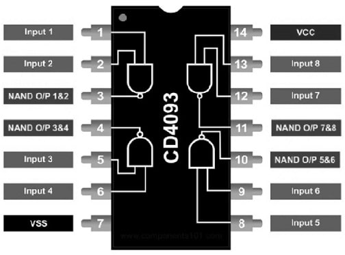
The pin configuration of CD4093 IC is shown below which includes 14 pins and each pin and its functionality is discussed below.

CD4093 IC Pin Configuration
- Pins – 1, 5, 8 & 12 (A1 to A4): These are Inputs-A pins of the four NAND gates.
- Pins – 2, 6, 9 & 13 (B1 to B4): These are Inputs-B pins of the four NAND gates.
- Pins -3, 4, 10 & 11 (Q1 to Q4): These are the output pins of the four NAND gates.
- Pin-14 (VDD): These are +3 to +15V voltage supply pins.
- Pin-7 (GND): It is a power GND pin (0V).
Features & Specifications:
The features and specifications of CD4093 IC include the following.
- Its logic family is CD4000.
- It belongs to the logic gates category.
- It has a NAND logic function.
- The logic type is CMOS.
- It includes four logic gates.
- The input type is Schmitt Trigger.
- Number of bits – 4-bits.
- The number of i/p lines it has is two Input & Number of o/p lines it has is one output.
- Its maximum o/p current is -1.5 mAmps.
- Its low range o/p current is 1.5 mAmps.
- Its propagation delay time is 380 ns.
- Its voltage supply ranges from 3 to 18V.
- Its operating current supply is 60 uA.
- The operating voltage supply is 10V.
- Its quiescent current is 40 nA.
- Its minimum and maximum operating temperature ranges from -55°C to +125°C.
- The mounting style is SMD or SMT.
- The package or Case is SOIC-14.
- Noise immunity is > 50%
- Input rise & fall times are unlimited.
CD4093 IC Working
The main feature of this IC is the Schmitt-trigger property at the input. So, current supplies through a couple of inputs. This integrated circuit exerts a time lag above the input voltage to avoid the pressure of a stray input signal. As a result, the output signal is proportional to the input current. Therefore, you will get only a genuine input pulse. In addition, the circuit utilizes a wide range of voltage supply. Therefore, you can generate a high output based on the strength of the input signal.
It is also known as the NOT-AND gate and it works as; whenever the inputs are true then it provides a false output. So it is the complement o/p of AND gate. This is a 14-pin IC that includes 4 NAND gates internally. The inputs of the NAND gate 1 are Pin(1) A & Pin(2) B which provides a complement AND gate output at pin(3).
The inputs & the output of the NAND gate are shown in below truth table below. If any inputs are provided to pins 1, 2, 5, 6, 8, 9, 11 & 12 then an equivalent output throughout the NAND gate will be obtained. So the below table can be referred to for the input & output values.
IC 4093 Schmitt trigger is a unique type of NAND gate, so one of its most important features is how fast it responds to incoming signals. Logic gates with Schmitt trigger activate and turn ON their outputs low or high only when their input logic level achieves a genuine level which is known as hysteresis. The ability of Schmitt triggers to make hysteresis is a fundamental feature.
Equivalent & Alternatives
Equivalent CD4093 IC are; NTE4093, HCF4093, 7400, SN74LVC1G132DCKR, 7420, MC14093, HEF4093 or TC4093 and an alternate CD4093 IC is 74HC132.
Micro Flasher Circuit with CD4093 IC
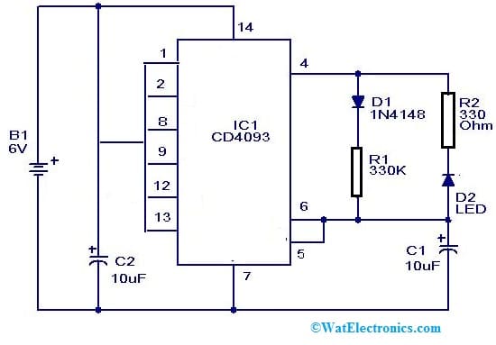
This micro flasher with CD4093 IC circuit is shown below which emits a flashing light continuously with very less power consumption. This simple circuit runs with four 1.5 V torch cells for a very long time.
The required components to make this circuit mainly include CD4093 IC, LED, 1.5 V cells, 1N4148 Diode, 330K, 220Ohms, and capacitors like; 100u 16V and 10u 16V. Connect the circuit as per the micro-flasher circuit diagram shown below.

Micro Flasher Circuit with CD4093 IC
Working
Generally, the human brain and eye react sharply to unexpected changes in light intensity, particularly the flashing light. So a flashlight for a 10 ms time is essential for awareness at complete brightness. The brain or retina ability which is known as persistence of vision’ keeps the vision memory for a 20 ms period after that it fades slowly. The human eye detects the flashing light only as individual flashes if the gap between flashes is > 20 ms.
A low-power CD4093 CMOS IC is utilized to produce sharp flashes from the very bright red LED. Here LED is connected in such a way that it gets the current supply from the C2 storage capacitor. So this helps in reducing the battery drain as LED is not powered directly from the IC output.
The R1 resistor value decides the current drain using the battery to charge the C2 capacitor. The current drain is approximately 18 µA with the given 330 kilo-ohms value and the R2 resistor limits the flow of current throughout LED.
This circuit is not expensive and can be designed on a tiny perforated board. In a small case, it must be enclosed with a front panel which is similar to a burglar alarm so that LED flashing provides an alarm. For an eye-catching appearance, use a transparent and high-brightness LED in the circuit. The flasher is used as a pathfinder within exit doors or corridors whenever power fails.
Beeper circuit with CD 4093 IC
Generally, some electrical devices we come across generate a small beeping sound continuously when they are switched like heaters, computers, microwaves, LCD TVs, etc. But these beeping signals are only just a second (or) two long enough. In addition, the beeping sound can also act as a reminder within several gadgets.
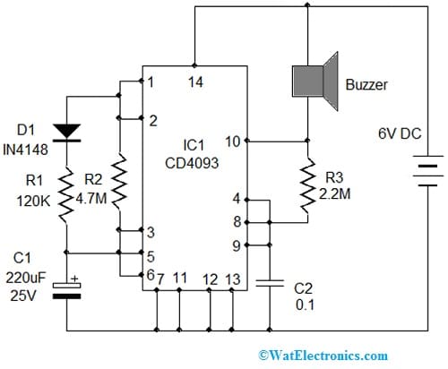
The beeper circuit with CD 4093 IC is shown below which can be used as a power-on reminder if heavy current devices are turned ON. For every five minutes, it generates a short beep sound to remind the power-on condition.
The required components to make this beeper circuit mainly include; resistors like; 120K, 4.7M, & 2.2M, capacitors like; 470 uF 25 V and 0.1, IN4148 diode, CD4093 IC, 6V power supply, and a buzzer.

Beeper circuit with CD 4093 IC
Working
The CD4093 CMOS IC is used as a simple oscillator with its logic gates. R1 & R2 resistors & C1 capacitor determines the ON/OFF time of the oscillator. The Off time is approximately 5 minutes with the given R2 & C1 values. The ON time is approximately 2 seconds with the R1 value. So this timing can be modified by changing the R1, R2 &C1 values. If the R2 value is high, then the OFF time will be higher. If the R1 value is low, then the ON time will be very low. Here C1 value decides the whole ON/OFF oscillator timing.
This beeper circuit can be worked with a 6V adapter power supply. So if this circuit is utilized as a power-on reminder, then AC to the power supply must be tapped using the power lines of the device to be checked. Thus whenever the switch activates then both the power supply and the device of the beeper receive power.
Advantages & Disadvantages
The advantages of CD4093 IC include the following.
- Schmitt-trigger inputs allow the integrated circuit to tolerate slow-falling or slow-rising input signals to make it more resistant to noise & provide constant switching.
- This IC has less power consumption which makes it suitable in low-power and battery-powered applications.
- This IC is commonly utilized in applications wherever logical NAND operations including Schmitt trigger inputs are necessary.
- It operates on different voltage levels & consumes 1uA of a maximum current whenever it is operated at 18Volts DC.
- These are a unique type of NAND gates, so one of the main useful features of this IC is how fast they respond to incoming signals.
- The Schmitt trigger feature of this IC provides noise immunity & ensures very clean signal transitions to make it appropriate for applications with varying or noisy input signals.
The disadvantages of CD4093 IC include the following.
- The main drawbacks are; efficiency trade-offs, power handling, design complexity, and frequency range.
- CMOS circuits have turn into more vulnerable to leakage current, thus it can lead to increased heat dissipation and power consumption.
- These ICs are susceptible to errors occured by ionizing radiation, so that can be a problem in certain space systems applications.
- The power consumption & high transistor density in advanced CMOS ICs can make important thermal management challenges, thus needing advanced cooling solutions.
- As CMOS technology scales, the fabrication process becomes increasingly complex, requiring more advanced manufacturing equipment and processes.
- These are static sensitive, so touching a pin when charged with static electricity may harm the IC.
Applications
The applications of CD4093 IC include the following.
- The CD4093 IC is used commonly in digital logic circuits, pulse generators, oscillators, and applications wherever Schmitt triggers are helpful like; in handling noisy signals or debouncing switches.
- This IC is used in pulse shaping, signal conditioning, oscillator circuits & also a variety of digital logic circuits.
- These are used in wave & pulse shapers; astable multivibrators, monostable multivibrators; and high-noise-environment systems.
- It is used in NAND logic implementation.
Please refer to this link for the CD4093 IC Datasheet.
Thus, this is an overview of CD4093 IC, pinout, specifications, circuit, working, and its applications. This IC has four separate two-input NAND logic gates where each gate is set with Schmitt-trigger inputs. Schmitt trigger provides hysteresis within the input signal to make them mainly useful within applications wherever signal or noise bouncing may take place. This IC has typically 14 pins like power supply pins like VDD & VSS, input pins like; A & B for every gate, and output pins like Q for every gate & other control pins. Here is a question for you, what is CD 4017 IC?