In digital electronics, a flip-flop is a digital electronic circuit that includes two stable states that are used for storing binary data. This data can be modified by simply applying varying i/ps. Flip-flops are basic data storage elements and basic building blocks in digital electronics systems utilized in communications, computers & different types of systems. There are different types of Flip Flops available in digital electronics like SR, JK, D & T. This article discusses one of the types of Flip Flop IC – CD4027 JK Flip Flop, pin configuration, working, and its applications.
What is CD4027 JK Flip Flop?
The CD4027 IC is a CMOS-based high-speed dual JK Flip-Flop. This IC includes two same JK flip flops and each JK flip flop pair in this IC includes provision of J, K, pins, set, reset with clock & two o/p terminals. This Flip-Flop IC operates normally at 16MHz speed at 15V high voltages with only 2.5V of low noise margin.
These FFs can be used in different applications to store data which includes counters, a control circuit & voice register. This IC performs different functions like register, control & toggle. These flip-flops are known as latching devices so it remembers one single data bit & latches the o/p depending on it. So because of this property, these ICs are normally commonly used as control registers, shift registers, storage registers, or wherever ever a small memory is necessary.
Pin Configuration:
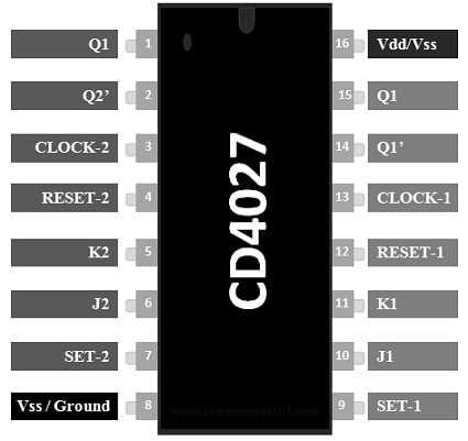
The CD4027 JK Flip Flop pin configuration is shown below. This flip flop includes 8 pins and each pin and its functionality is discussed below.

CD4027 JK Flip Flop Pin Configuration
- Pin16 (Vcc): This pin powers the chip with 5 volts.
- Pin8 (Ground): This is a GND pin, connected to the GND of the system.
- Pins 3, 13 (CLK-1/ CLK-2): These two pins should be provided by CLK pulse for the FF.
- Pins 2, 7 (Reset-1 / Reset-2): Once the Preset is high then the FF will set Q=1 & not Q=0.
- Pins 4, 12 (Clear-1/Clear-2): Once Clear is high then FF will set Q=0 & not Q=1.
- Pin 5, 11 (K-1/ K-2): The Flip Flop’s input pins.
- Pins 6, 10 (J-1 / J-2): The FFs another i/p pins.
- Pins 2,14 (Q-1’ / Q-2’): Inverted o/p pins of FF.
- Pins 1,15 (Q1 / Q2): These are o/p pins of the FF.
Features & Specifications:
The features and specifications of CD4027 JK Flip Flop include the following.
- It is a Dual JK FF IC.
- Its operating speed is 16MHz.
- Its operating voltage is 5V/10V/15V.
- Its max operating voltage is 20v.
- Input Rise or Fall time at 5V is 45us.
- High Range i/p voltage min is 2V.
- The low-level i/p voltage max is 0.8V.
- It is available in 14-pin packages like GDIP, PDIP & PDSO.
- This IC operates at 16 MHz medium speed normally through a 10V supply.
- Its voltage supply ranges from 3.0V – 15V.
- The operation of FF is static.
- Typical noise immunity is high like 0.45 VDD.
- It has a Set & Reset ability.
- It is compatible with TTL.
- It has typically 50 nW of low power.
- Alternative CD4027 JK Flip Flops are; 74LS73, CD4013B, 74LS76, CD4095, CD4043 & CD4042
IR Remote Control Switch Circuit with CD4027 JK Flip Flop
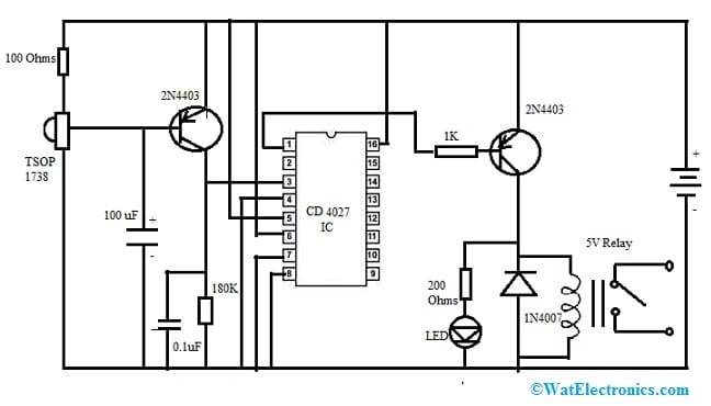
Earlier remote controls were very complex & huge but at present, these were developed very simply using few components with various technological advances. The IR remote control switch circuit with cd4027 jk flips flop is shown below. This circuit is very helpful in connecting any appliance to switch them ON & OFF like lamp, fan, light, etc.
The required components to make this IR remote control switch circuit mainly include a breadboard, 5V battery, TSOP 1738 IR sensor, Q1-N4403, Q2-2N4403 transistors, CD 4027 J-K Flip-flop IC, 5V Relay, 1N4007 Diode, LED, Resistors like 100Ω, 200Ω, 180KΩ & 1KΩ and capacitors like 100µF & 0.1µF. Connect the circuit as per the connections shown in the diagram.
The most significant components of this remote control switch circuit are TSOP 1738 IR sensor & CD4027 J-K flip flop IC. The TSOP 1738 IR sensor gets 38 KHz of IR signals. This sensor includes a PN photodiode & a preamplifier stage within it and the JK flip-flop works like a toggle switch.

IR Remote Control Switch Circuit with CD4027 JK FF
Working
This circuit works with 5 volts supply. The IR sensor in this circuit receives a 38 KHz IR signal. This signal is transmitted to a Q1 transistor for signal amplification. After that, this amplified signal goes to the CLK- 2 pins of the Flip Flop IC. The output of this IC will give voltage to the Q2 transistor so that it activates. This Q2 transistor enables the 5V relay which is connected to it. Once the relay triggers, an LED will turn ON. So any appliance can be connected with this relay directly to turn on & off through this circuit.
This IR remote control switch with CD4027 JK FF can be used as a switch to control different home appliances like lights, fans, TV, AC, CD or DVD player, etc. From the above circuit, we can know how to connect a CD4027 JK Flip Flop.
Generally, JK Flip flops are used in the remote control circuit to address :
Debouncing: Remote control buttons or switches can sometimes produce noisy or unstable signals due to mechanical vibrations or bouncing contacts. The J-K flip-flop, when properly configured, can help stabilize the input signals by providing a debouncing effect. It ensures a stable and reliable signal is generated when a button or switch is pressed.
Synchronization: In remote control systems, it is crucial to ensure that the transmitted signals are synchronized and consistent with the desired functionality. The J-K flip-flop can be used to synchronize and control the timing of signals in the remote control circuitry. This helps in ensuring that the transmitted signals are interpreted correctly by the receiving end.
Memory: The J-K flip-flop has memory elements that can store information. In remote control applications, it can be used to store the state or status of buttons or switches. For example, when a button is pressed on a remote control, the J-K flip-flop can latch the state and maintain it until another button is pressed. This allows for sequential operations or the control of different functions within the remote control system.
Control and Logic: The J-K flip-flop can be combined with additional logic gates to create more complex control and timing circuits. This allows for the implementation of various features and functions in remote control systems, such as mode selection, channel switching, or other user-defined operations.
The choice of flip-flops depends on the specific requirements and functionality of the remote control application. Different flip-flops like D flip-flop, T flip flop or SR flip-flop can also be used but each offers its own varying features and capabilities, allowing designers to select the most suitable one for their particular use case.
Where to use CD4027 JK Flip Flop/Applications:
The applications of CD4027 JK Flip Flop include the following.
- It is used in the memory circuits of computers.
- This flip-flop plays a key role in designing shift registers because they are sequential logic circuits mostly used for storing digital data.
- It is used in Memory or voice registers & control registers because of its latching property.
- It is used in EEPROM circuits to hold a small amount of data.
- This CD4027 JK FF IC is mainly used to store data & also to perform register, toggle & control functions.
- This IC is used to change the signal through control i/ps within toggling applications.
- This FF can be used in latching devices because of its storing data property & determines the o/p depending on the previous o/p.
- The CD4027 JK flip flop IC includes two JK flip flops where each FF can be used based on the application individually.
- The CD4027 JK Flip Flop is used to design a synchronous binary counter.
- It can be used as a frequency divider.
- It is used in digital circuits.
- IC 4027 could be used to produce pulse width modulated (PWM) signals.
- A circuit that uses frequency modulation, or the act of changing a signal’s frequency to transfer information, may be created using the IC 4027.
- This 4027 IC is often used in sequential logic circuits, which have counters, shift registers & frequency dividers.
- These ICs are also used to make oscillator circuits to produce periodic signals with a particular frequency.
Please refer to this link to 74LS74 D Flip Flop Datasheet, CD4014 Shift Register Datasheet.
Please refer to this link to know more about CD4027 JK flip flop Datasheet.
Thus, this is an overview of a CD4027 JK flip flop–pin configuration, specifications, circuit, and working with applications. This CD4027 JK flip-flop IC is best for latching purposes and also it works like a small programmable memory in many projects. Here is a question for you, what is a latch?