In digital electronics, universal gates like NAND and NOR plays a key role because these gates implement any Boolean function. So, the NAND logic gate is one kind of digital logic gate used most frequently in digital logic design applications. In CMOS logic, there are different types of NAND gate ICs like CD4011, CD4023 & CD4012. So, CD4012 IC is a four-input NAND gate IC, designed with the monolithic CMOS. This IC size is compact & interfaced easily with CMOS NMOS & TTL devices. This IC provides a wide range of features like ESD barring & high noise immunity. This article provides brief information on CD4012 dual 4-input NAND gate like features, specifications, circuit, and its applications.
What is CD4012 Dual 4-Input NAND Gate?
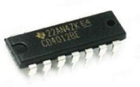
The CD4012 is a 4-input NAND gate based on CMOS technology. This IC is available in a Dual package which means it includes two NAND logic gates where each gate has four inputs. So these gates can function independently. This IC belongs to the CD4000 series and it has a wide range of voltage supply and uses less power. This NAND gate IC is commonly used in logic inverter circuits, buffer circuits, and many more.

CD4012 IC
CD4012 IC Pin Configuration:
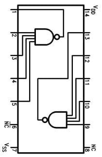
The pin configuration of the CD4012 dual 4-input NAND gate is shown below. This IC includes 14 pins which are discussed below.

CD4012 IC Pin Configuration
- Pin1 (Q1): It is an output pin of the first NAND gate.
- Pins 2, 3, 4 & 5 (A1, B1, C1 & D1): These pins are input pins of the first NAND gate.
- Pins 6,8 (Not Connected): These are not connected pins.
- Pin7 (GND): It is a ground pin of the IC.
- Pins 9,10,11 & 12 (A2, B2, C2 & D2): These are input pins of the second NAND gate.
- Pin13 (Q2): It is an output pin of the second NAND gate.
- Pin14 (VDD): It is a 5V power supply pin.
Features & Specifications:
The features and specifications of CD4012 IC include the following.
- It is a Dual NAND gate IC.
- The logic family is CD4000.
- The logic function is NAND.
- The type of logic is four Input NAND gates.
- No. of Bits is 2 bit
- It includes two logic gates.
- It has four inputs and a single output.
- The propagation delay time is 250 ns.
- The operating current supply is 15 uA.
- Quiescent current is 20 nA.
- Operating temperature ranges from -55 ~ +125°Centigrade.
- The mounting style type is through the hole.
- It is available in 14-pin GDIP, PDSO & PDIP packages.
- The range of operating voltage is 3V to 15V.
- Buffered inputs & outputs by operating voltage – 5V.
- Its power dissipation is 500mWatts.
- Protection of diode on all inputs.
- Maximum propagation delay is 50ns at 10Volts.
- Minimum low & high logic voltage ranges from 0.05V – 4.95V.
- Equivalents CD4012 ICs are 74S140 and 74HC20 whereas other logic gates are; 74LS00, 74LS04, 74LS08, 74HCT04 & 74LS02.
CD4012 IC Working
The CD4012 NAND gate IC operation is very simple. This logic gate function is opposite to AND logic gate. The function of the NAND gate for two inputs is. When any of the inputs is low, then it gives high output. When the values of both the inputs are HIGH, then it provides LOW logic output ‘Z’ is given below. The logic function for this gate is Z = (XY)’.
|
X |
Y |
Z |
|
L |
L | H |
|
L |
H | H |
| H | L |
H |
| H | H |
L |
Similarly, let us consider CD4012 IC which includes four inputs namely X, Y, Z Q & the output as S. The output S will follow the logic expression S = X, Y, Z Q. The truth table for four input NAND gates is shown below. The logic function is S = (X, Y, Z Q)’.
| X | Y | Z | Q |
S |
|
L |
L | L | L | H |
|
L |
L | L | H | H |
|
L |
L | H | L |
H |
| L | L | H | H |
H |
|
L |
H | L | L | H |
| L | H | L | H |
H |
| L | H | H | L |
H |
|
L |
H | H | H | H |
| H | L | L | L |
H |
|
H |
L | L | H | H |
|
H |
L | H | L |
H |
| H | L | H | H |
H |
|
H |
H | L | L | H |
|
H |
H | L | H |
H |
| H | H | H | L |
H |
| H | H | H | H |
L |
Bedside Lamp Timer Circuit using CD4012 IC
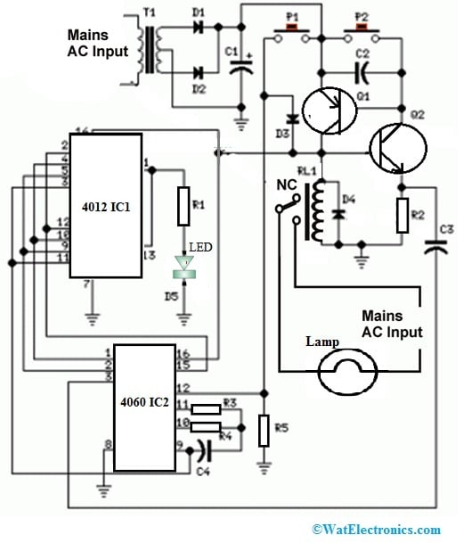
The bedside lamp timer circuit using CD4012 IC is shown below. This circuit is designed to turn ON a lamp otherwise any other appliance in 30 minutes & then to turn off it.
The required components to make this circuit mainly include; resistors R1-1K, R2- 4K, R3-10M, R4-1M, R5-10K, capacitors C1- 470µF-25V, C2-C4100nF-63V, C1-470µF-25V, C2-C4 is 100nF-63V, diodes from D1to D4-1N4002, D5-5mm. red LED, CD4012 IC1, CD4060 IC2, transistors Q1-BC328, Q2-BC547, P1 and P2 SPST pushbuttons, T1 transformer, RL1 – 10.5V 470 Ohm Relay with SPDT 2A 220V switch male mains plug – PL1 and female mains socket – SK1. Connect the circuit as per the diagram shown below.

Lamp Timer Circuit with CD4012 IC
In the above circuit, the transistors like Q1 & Q2 are opposite in characteristic. The. Q1 used in the circuit is an 800mA PNP BC328 transistor whereas the Q2 transistor used is a 100mA BC238 NPN transistor. In the above circuit, when the P1 push button activates, the relay RL1 will turn on then the two ICs are activated. The relay switch activates the lamp & IC2 will reset by a positive voltage at pin 12. Here, the IC2 oscillating frequency is determined by C4 & R4. The T1 time can be adjusted by changing the R4 & C4 value. Whenever the pin-3 of IC2 goes high after 30 minutes then this turns off the whole circuit through C3.
The LED blinks during those six minutes of alarm time at a frequency provided by the IC2 oscillator at pin-9. Here, IC1 is directly connected to pins 1, 2 & 15 of IC2 in the circuit. In IC1, the two NAND gates are parallel to enhance the current toward the blinker. The time can be changed by changing the R4 & C4 values. A Piezo buzzer is connected between pins 1 & 14 of IC1.
Working
This circuit is very useful frequently for a reader when he sleeps while reading then this circuit will turn off automatically after a specified time T1. In the circuit, the two push buttons P1 & P2 are connected through the bedside lamp. When the P1 push-button is pushed, the D5 LED will glow for 25 min that is the time of reading allotted. Before 6 minutes the LED blinking will be switched off for 2 min by generating an alarm to the person who reads that his/her reading time is getting finished. After that for 2 minutes, the LED stops blinking. After this time interval, again it starts blinking for two more minutes to indicate that the ON time has finished. If the reader needs to increase the reading time then it is necessary to push the P1 button once more and the reader at any point in time can be turned off by pushing the P2 button.
Where to use CD4012 IC/Applications
The applications of CD4012 IC include the following.
- These ICs are used in Digital Logic circuits to generate preferred logical functions.
- These NAND gate ICs used in Multiplexers, Encoders, De-multiplexers & Decoders.
- It is used in logic buffer circuits.
- These gates are used in oscillators, networking & digital systems.
- These are used in fundamental logic circuits.
- It is used in different fields like industrial controls, automotive, instrumentation, medical electronics, remote metering, data terminals, computers, alarm system, etc.
- This NAND logic gate can be utilized with other types of logic gates.
- This IC is used where multiple gates otherwise buffer circuits are required.
- It is applicable where high noise immunity & low dissipation are necessary.
- It is sued for digital implementation within logic circuits.
Please refer to this link for: CD4012 Dual 4-Input NAND Gate Datasheet.
Thus, this is an overview of the CD4012 dual 4-input NAND gate, pin configuration, specifications, working, and its applications. This NAND gate IC belongs to the series of CD4000 IC and it is designed with the monolithic CMOS IC. This IC is available in a 14-pin DIP hermetically sealed and it offers a wide range of features. These are compact & are interfaceable easily with CMOS, NMOS & TTL devices. Here is a question for you, what are the examples of AND gate ICs?