In digital electronic devices, like computers/processors, adders are the digital logic circuits designed for ALU operations such as the addition of 2 or more binary numbers, address calculation, address calculation, increment and decrement operations, counting, table indexes, etc. Because the bits flow and computation in these logic circuits ensure the performance, functionality, and performance of the computers. This article describes the 4-bit full adder that is available in CD4008 IC and used in many applications such as counters, binary addition, encoders, decoders, etc.
What is CD4008 IC?
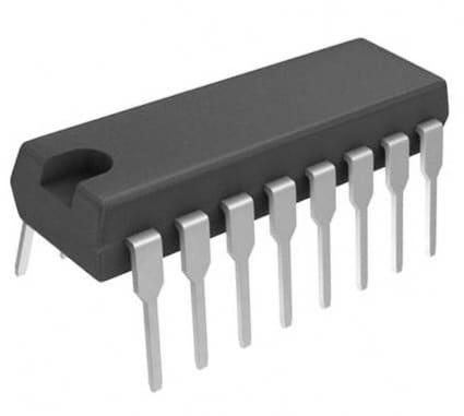
In smart machines, the CD4008 is a high voltage and high speed integrated circuit used to add two inputs of a 4-bit sequence with a high speed and high voltage parallel carry feature. It consists of 4-stages of full adders arranged independently in a single TO-92 package. It can perform arithmetic/binary operations with a fast transition of bits between stages, and a carry-in-carry-out feature.

CD4008 4-Bit Full Adder IC
That means. the circuit allows high-speed “parallel carry execution” to perform the high-speed operation in the arithmetic operations in ALU. It adds two inputs A, B of 4-bit sequences -A1, A2, A4, A4 and B1, B2, B3, and B4 with carry in CI and Carry Out CO to obtain 4-Bits of sum output S1, S2, S3, and S4. It is also known as CD4008BMS Or MC14008B 4-Bit full adder IC.
Instead of microcontrollers, the CD4008 multiples full adder ICs are used to perform binary addition operations to reduce the cost and complexity of circuit design. The 4 individual stages of full adder circuits are cascaded and integrated into a single chip to form a 4-Bit CD4008 full adder IC.
Pin Configuration of CD4008 IC:
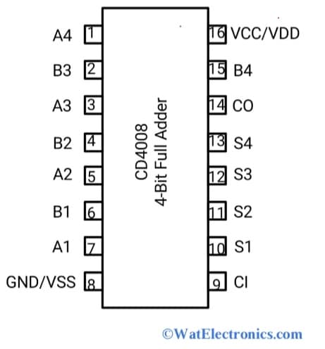
The CD4008 is a popular 16-pin 4-bit full adder integrated circuit used in arithmetic operations like addition. The pin configuration of the CD4008 IC is explained in the diagram shown below. This IC is integrated with 4 full adder circuit stages, which are independent.

Pin Diagram Of CD4008
Pin 1 & 15: A4 and B4: These pins refer to the inputs of the fourth NAND gate of the CD4008 4-bit full adder circuit.
Pin 2 & 3: A3 and B3: These pins are referred to as the inputs of the second NAND gate CD4008 4-bit full adder circuit.
Pin 4 & 5: A2 and B2: These pins are referred to as the third NAND gate CD4008 4-bit full adder.
Pin 6 and 7: A1 and B1: These pins are referred to as the inputs first NAND gate 4-bit full adder CD4008.
Pin 8: GND/VSS: This pin is referred to as the common ground connection, which represents 0V.
Pin 9: CI: This pin is referred to as the carry input of the first full adder. The carry output of the first full adder is given as the carry input to the second full adder and so on.
Pin 10: S1: This pin is referred to as the sum output obtained at the first full adder stage by addition.
Pin 11: S2: This pin is referred to as the second bit of the output obtained at the second full adder stage by addition.
Pin 12: S3: This pin is referred to as the third bit of the output obtained at the third full adder stage by addition.
Pin 13: S4: This pin is referred to as the fourth bit of the output obtained at the fourth full adder stage by addition.
Pin 14: CO: This pin is referred to as the high-speed parallel carry output bit obtained at the last full adder stage of CD4008.
Pin 16: VCC/VDD: This pin is referred to as the positive power input supply, which is given to operate the CD4008 IC. Its operating voltage is either 5V Or 10V Or 15V.
Technical Features and specifications Of CD4008 4-Bit Full Adder:
The following are the few features of the CD4008 Or CD4008BMS 4-Bit full adder with high-speed parallel carry out.
- It is a high-speed and high-voltage 4-Bit full adder IC manufactured in 16-pin CDIP, SOIC, PDIP, and TSSOP packages with a voltage rating of 20V.
- It generates four outputs of addition/sum and look ahead parallel carry output.
- Its typical operation time @VCC=10V & CL=50pF is 160 nsec for Sum-In-to-Sum-Out and 5 nsec for Carry-In-To-Carry-Out.
- It generates standardized symmetrical output characteristics.
- It is performance is tested 100% at 20V rating for quiescent current.
- It generates high-speed parallel carry output.
- The maximum input current over a full package temperature range at 18V is 1 microamp.
- The maximum input current at 25°C and 18V is 100nAmps.
- Meets all standard specifications and requirements of B series CMOS devices.
- Its normal operating voltage ranges 5V, 10V, and 15V.
- The maximum operating voltage is 20V.
- The noise margin at 5V operating voltage is 1V.
- The noise margin at 10V operating voltage is 2V.
- The noise margin at 15V operating voltage is 2.5V.
- The low input voltage is 1.5V maximum.
- The high input voltage is 3.5V minimum.
- The range of operating temperature is -55°C to +125°C.
- The range of storage temperature is -65°C to +150°C.
- The lead temperature is +265°C.
Working of CD4008 4-bit Full Adder
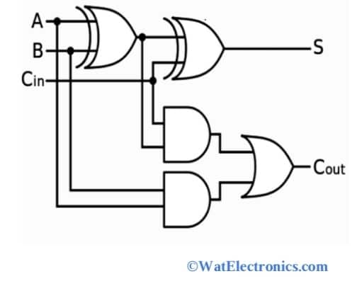
The CD4008 4-bit full adder IC is a combination logic IC with 4 individual full adder stages cascaded in a single package. To understand the working of this full adder, consider the following full adder logic circuit diagram using logic gates.

Logic Circuit Of 4-Bit Full Adder
The logic circuit is designed with 2 XOR gates, 2 AND gates, and 1-OR gate. The first XOR gate adds the two given inputs A and B in binary form 0 or 1 along with the carry-in bit and the added/sum output is obtained from the 2nd XOR gate. The final carry output is obtained from the OR gate. The 2 AND gates are used to add the carry bits of the previous full adder stage to the next full adder stage to obtain the final output carry bit from the OR gate. That means, the OR gate and the 2nd XOR gate generate the sum output and carry output bits based on the given inputs and carry bits of previous stages.
The above logic circuit is for the 1-bit full adder stage in the CD4008. In the same way, the 4-stages of full adder circuits are integrated into an IC to form a 4-bit full adder. Hence, the CD4008 4-bit full adder IC was designed by arranging it in such a way that the output carry of the first full adder stage becomes the input carry of the next full adder stage and so on. From the last (4th) full adder stage we get the high-speed output to carry bit CO and the final sum output S (S1, S2, S3, S4).
CD4008 4-bit Full Adder with High-Speed Parallel Carry:
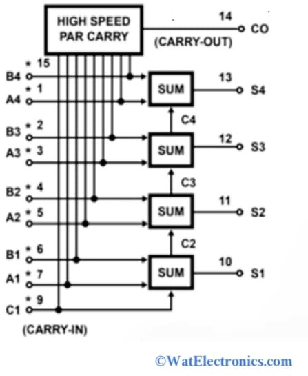
The inputs of the CD4008 4-bit full adder IC are protected by the CMOS protection network. The block diagram shown below explains the internal working of CD4008 4-bit full adder IC.

Internal Block Diagram Of CD4008
From the above block diagram,
- A1 is the input bit of the first full adder circuit
- A2 is the input bit of the second full adder circuit
- A3 is the input bit of the third full adder circuit
- A4 is the input bit of the fourth full adder circuit
- CI or C1 is the carry input of the first full adder circuit
- CO is the high-speed parallel carry output bit of the CD4008.
- S1 is the sum output of the first full adder circuit
- S2 is the sum output of the second full adder circuit
- S3 is the sum output of the third full adder circuit
- S4 is the sum output of the fourth full adder circuit.
- C2, C3 and C4 are the carry-out bits of the second, third and fourth full adder stages.
The truth table of the CD4008 4-bit full adder is shown below.
| Input A= A1, A2, A3, A4 | Input B=B1, B2, B3, B4 | Carry-In (CI) | High-speed parallel carry CO | Sum (S) =
(S1, S2, S3, S4) |
| 0 | 0 | 0 | 0 | 0 |
| 1 | 0 | 0 | 0 | 1 |
| 0 | 1 | 0 | 0 | 1 |
| 1 | 1 | 0 | 1 | 0 |
| 0 | 0 | 1 | 0 | 1 |
| 1 | 0 | 1 | 1 | 0 |
| 0 | 1 | 1 | 1 | 0 |
| 1 | 1 | 1 | 1 | 1 |
In the CD4008, the adder obeys the above truth table for the given input data. As we know, the internal structure of CD4008 is a combination of four complete full adder circuits connected in series. The first full adder stage takes two inputs A1 and B1 with the carry-in bit from a different user or device. Initially, the carry-in bit of the first full adder stage will be binary ‘0’.
The carry-out obtained from the addition of two inputs acts as a carry-in bit to the preceding full adder stages. Finally, the last full adder stage gives the high-speed parallel carry-out bit from the addition of 4-bit input values. The CD4008 4-bit full adder circuit starts adding the input bits from the LSB and continues adding to the MSB. As the carry bits are transferred to the preceding full adder stages, the carry-out issue during addition can be solved easily.
The block diagram of the CD4008 4-bit full adder with high-speed parallel carry output bit is shown in the figure below.
From the above block diagram, the CD4008 contains 4 individual stages of a full adder circuit and every stage of the circuit contains two input values along with the carry bit. The sum output will be either logic high (1) or logic low (0) based on the values given on the CD4008 input pins. If the carry is obtained during the addition, then it represents logic High (1). Otherwise, it will be logic low (0). To verify the above truth table in simulation, then follow the below steps.
- When all the inputs are logic ‘0’ and the carry-in is logic ‘0’, then the sum S output will be logic ‘0’ and the carry-out CO will also be ‘0’.
- If any one of the inputs is high (1) and the carry-in bit is ‘0’, then the sum output S will be high (1) and the carry-out will be low (0).
- If all the inputs are high (1) and carry-in is low (0), then the sum output will be low (0) and the carry-out will be high (1).
- If any one of the inputs is high (1) and the carry-in bit is high (1), then the sum output will be low (0) and the carry-out CO will be high (1).
- If all the inputs are low (0), carry-in CI is high (1), then the sum output S will be high (1) and CO will be low (0).
- If all the inputs are high (1), carry-in CI is high (1), then the sum output and CO will be high (1).
Therefore, multiple CD4008 4-bit full adders can be implemented very easily in complex logic circuits for arithmetic operations instead of single full adder circuits.
Applications Of CD4008 4-Bit Full Adder:
The following are the applications of the CD4008 4-bit full adder,
- Used in circuits for fast binary additions or arithmetic operations.
- Used in arithmetic and logic units (ALUs).
- Used in mini calculators.
- Used in counters.
- Used in logic circuits.
Please refer to this link to know more about CD4008 IC Datasheet.
Thus, this is all about an overview of the CD4008 4-Bit full adder. The alternatives are 74LS483, MC14008, and NTE4008 full adders. There is a chance to expand the 4-bit full adder to an 8-bit full adder by cascading two CD4008 4-bit full adder ICs for some complex arithmetic operations and complex logic designs. Make sure that the input values don’t get shuffled. Because the obtained output sum depends on the given input bit sequence. Here is a question for you, what is a half adder?