We all know that in the current day technology everything becomes digitized and digital systems are designed based on fundamental configurations like AND, OR, and NOT gate. These configurations are employed in multiple network designs. Apart from performing logical functionalities, systems should also store up binary numbers and for storage purposes, Flip Flop’s are invented. So, for some functionalities, the combination of Flip Flop’s and logic gates are used, and IC’s (Integrated Circuits) are developed. These integrated circuits are the functional blocks of digital systems and one of the ICs today we are going to discuss is the carry-lookahead adder. This article explains on carry-lookahead adder circuit, its truth table, architecture, used, and benefits.
What is Carry Lookahead Adder?
This is a kind of electronics adder that is mainly employed in digital logic. A carry-lookahead adder is also called a fast adder that augments the speed required for determining carry bits. We know that a computer performs its activities through arithmetic operations such as division, addition, multiplication, and subtraction. So, a division is repeated subtraction, and multiplication is repeated addition correspondingly.
In order to perform these repeated functions, adder circuits are required and those are half adder, full adder, carry lookahead adder.
A carry lookahead adder definition is it is the faster circuit in performing binary addition by using the concepts of Carry Generate and Carry Propagate. A CLA is termed as the successor of a ripple carry adder. A CLA circuit minimizes the propagation delay time through the implementation of complex circuitry.
The operation of carry lookahead is based on two scenarios:
- Calculate every digit position to know whether that position is propagating a carry bit that comes from its right position.
- Then combine the calculated values to produce the output for every set of digits where the group generates a propagation bit that comes from the right position.
Block Diagram
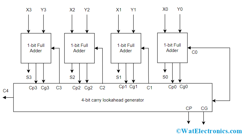
Carry lookahead adders operate by generating two bits called Carry Propagate and Carry Generate which are represented by Cp and Cg. The Cp bit gets propagated to the next stage and the Cg bit is used for generating the output carry bit and this is independent of the input carry bit. The below picture shows the 4-bit carry lookahead adder architecture.

4-bit Carry Lookahead Adder Architecture
The total number of gate levels in the circuit for carry propagation can be known from the full adder circuit. From input Cin to output Cout, two gates are required which are AND and OR gates. As w are considering a 4-bit circuit, the total number of gate levels will be 8. In the same way, for an n-bit parallel adder circuit, there is a 2n number of gate levels.
For the construction of carry lookahead adder, we need two Boolean expressions which are for carry lookahead adder formula for carry propagate Cp and carry generate Cg.
Cpi = Xi ꚛ Yi
Cgi = Xi . Yi
With the above expressions, the sum and carry at the output can be given as:
Sumi = Cpi ꚛ Ci
Ci+1 = Cgi + (Cpi . Ci)
With the above fundamental equations, the boolean expression for carry output at every stage can be known. So
C1 = Cg0 + (Cp0 . C0)
C2 = Cg1 + (Cp1 . C1) = Cg1 + (Cp1 . [Cg0 + (Cp0 . C0)])
- Cg1 + Cp1 . Cg0 + Cp1 . Cp0 . C0
C3 = Cg2 + (Cp2 . C2)
- Cg2 + (Cp2 . [Cg1 + Cp1 . Cg0 + Cp1 . Cp0 . C0])
C4 = Cg3 + (Cp3 . C3)
- Cg3 + (Cp3 . Cg2 + (Cp2 . [Cg1 + Cp1 . Cg0 + Cp1 . Cp0 . C0])
As per the above equations, the carry bit of any stage is based on:
Bits those are added in preceding stage and the carry bit that was provided in the initial stage.
Based on the C0, C1, C2, and C3 equations, the carry lookahead adder truth table is represented as follows:
| X | Y | Ci | Ci+1 | Condition |
| 0 | 0 | 0 | 0 | Carry generate will not be there |
| 0 | 0 | 1 | 0 | |
| 0 | 1 | 0 | 0 | |
| 0 | 1 | 1 | 1 | Carry propagate will not be there |
| 1 | 0 | 0 | 0 | |
| 1 | 0 | 1 | 1 | |
| 1 | 1 | 0 | 1 | Carry generate |
| 1 | 1 | 1 | 1 |
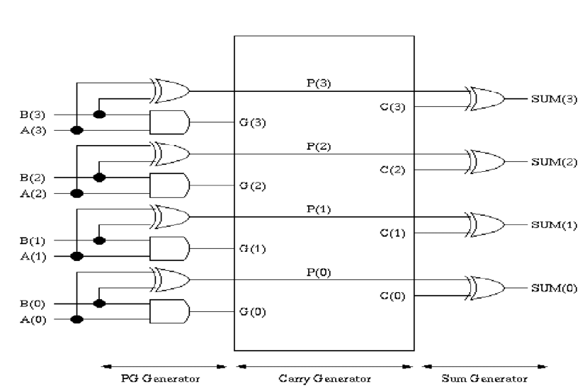
Also, the equations are applied using AND and OR gates which gives the carry lookahead adder circuit diagram.

Carry Lookahead Adder Circuit Diagram
Carry Lookahead Adder ICs
The CLA’s are combined with many ICs in multiple bit configurations. There exist various individual carry generator integrated circuits and these have to be connected with logic gates to execute addition operation.
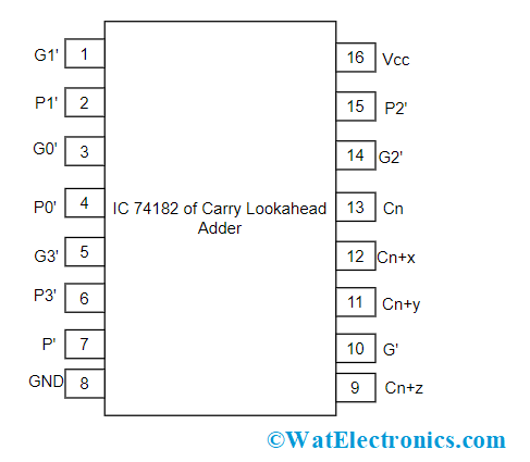
The IC for carry lookahead generator is IC 74182 where it accepts Po, P1, P2, and P3 as carry propagate bits inactive low condition and Go, G1, G2, and G3 as carry generate bits and Cn bit as active high input. The active high input pin generates high carriers (Cn+x, Cn+y, Cn+z) at all the stages of binary adders. The pin diagram of the IC is shown below:

Pin Diagram of IC 74182 CLA
Also, there is another highly performing adder ICs that integrate carry lookahead adder with a set of full adders. One of these types of IC is 74LS83. It is a 4-bit parallel adder that has four interconnected full adders along with wit CLA circuitry.
Ripple Carry Adder V/S Carry Lookahead Adder
There are many factors to be considered to know the difference between carry look ahead adder and ripple adder.
Propagation Delay
In the ripple carry adder, the carry bit ripple through every stage in the adder circuit and the time required for the carry bit to propagate from first to last bit is termed as propagation delay. So, the adder requires more time in computing the sum as the carry has to propagate till the last stage.
On basis of this, a carry lookahead adder was designed. Here, the sum of all bits that happened at a time without waiting for the previous stage additions.
So, CLA has minimum propagation delay when compared with RCA so the performance speed of CLA exceeds RCA. This is because of the correspondingly lesser critical path of CLA than RCA.
Dynamic Power Dissipation
When the temperature level is increased, both ripple carry and carry lookahead adders will have an increase in power dissipation at a linear exponential rate. On the other hand, the power dissipation also increased in RCA and CLA when Vdd is increased. From 0.6 V to 1.8 V, the power dissipation rate increases for both high-to-low and low-to-high scenarios.
A carry lookahead adder has minimal power dissipation when Vdd lies between 0.6 V to 0.9 V. At the range of 1.8 Volts, carry lookahead device shows maximum dissipation value which corresponds that lesser Vdd systems that use CLA has high performance and power dissipation also.
Static Power Dissipation
When the temperature level is increased, both ripple carry and carry lookahead adders will have a gradual increase in power dissipation at a linear exponential rate. When the Vdd value increases, then there will be a more exponential increment in the power dissipation.
In the range of 0.6 V to 1.8 V, there will a magnitude difference of five orders in the dissipation. Whereas at a Vdd of 1.8 V, the values of static power dissipation for RCA and CLA are almost same. And in the range of 0.6 V to 0.9 V, ripple carry adder holds a minimal value of power dissipation.
RCA manufacturing and designing is cheap, whereas the manufacturing procedure for CLA is costly than any other system.
The chips of RCA have significant size and area and in the CLA device, the chip area will increase when the number of components in the device increase.
The design of RCA and simple and repetitive. Carry lookahead adder has a somewhat complex design with more logic gates.
The computational speed and performance of RCA are slow whereas in CLA the computations can be done very quickly.
Cascading of CLAs
In order to get the addition of higher-order bits, it is required to cascade CLA adders. To design either 8-bit, 16-bit or 32-bit parallel adders, then the required number of 4-bit carry lookahead adders can be added using the carry bit.
For example, an 8-bit carry lookahead adder circuit diagram can be drawn and implemented using two 4-bit adders with additional gate delays. In a similar manner, a 32-bit CLA is formed by cascading two 16-bit adders thus forming a single system.
Verilog Code of CLA
The below example explains the 4-bit carry lookahead adder verilog code.
When two adder inputs are added, the output is one bit more than the inputs provided to both the adders.
Verilog Code:
include “full_adder.v”
module 4_bit_carry_lookahead_adder
(
input [3:0] sum1,
input [3:0] sum2,
output [4:0] result_output
)
wire [4:0] w_C;
wire [3:0] w_Cp, w_Cg, w_ADD;
full_adder FA_bit_0
(
.i_bit1(i_sum1[0]),
.i_bit2(i_sum2[0]),
.i_carry(w_C[0]),
.o_sum(w_ADD[0]),
.o_carry()
);
full_adder FA_bit_1
(
.i_bit1(i_sum1[1]),
.i_bit2(i_sum2[1]),
.i_carry(w_C[1]),
.o_sum(w_ADD[1]),
.o_carry()
);
full_adder FA_bit_2
(
.i_bit1(i_sum1[2]),
.i_bit2(i_sum2[2]),
.i_carry(w_C[2]),
.o_sum(w_ADD[2]),
.o_carry()
);
full_adder FA_bit_3
(
.i_bit1(i_sum1[3]),
.i_bit2(i_sum2[3]),
.i_carry(w_C[3]),
.o_sum(w_ADD[3]),
.o_carry()
);
// Creation of carry generate terms
assign w_Cg[0] = i_sum1[0] & i_sum2[0];
assign w_Cg[1] = i_sum1[1] & i_sum2[1];
assign w_Cg[2] = i_sum1[2] & i_sum2[2];
assign w_Cg[3] = i_sum1[3] & i_sum2[3];
// Creation of carry propogate terms
assign w_Cp[0] = i_sum1[0] | i_sum2[0];
assign w_Cp[1] = i_sum1[1] | i_sum2[1];
assign w_Cp[2] = i_sum1[2] | i_sum2[2];
assign w_Cp[3] = i_sum1[3] | i_sum2[3];
// Creation of carry terms
assign w_C[0] = 1’b0 // no carry input at first stage
assign w_C[1] = w_Cg[0] |(w_Cp[0] & w_C[0]);
assign w_C[2] = w_Cg[1] |(w_Cp[1] & w_C[1]);
assign w_C[3] = w_Cg[2] |(w_Cp[2] & w_C[2]);
assign w_C[4] = w_Cg[3] |(w_Cp[3] & w_C[3]);
assign result_output = { w_C[4], w_ADD};
endmodule
Carry Lookahead Adder Advantages and Disadvantages
The advantages of CLA are:
- Carry lookahead adder is considered as the fastest adder when compared with other adder systems.
- Here, the propagation delay is minimum because the output carry bit is only based on the first carry bit which is applied at the input stage.
- Using the equations of carry propagate, carry generate and carry bits, CLA devices generate carry-in for every adder in a simultaneous manner.
The disadvantages of CLA are:
- When the number of variables gets increased, the design of carry-lookahead adder becomes more complex.
- So, when the variables get increased and when CLA is integrated with IC, the area is required to increase.
- As the hardware is more, the circuitry cost becomes expensive when compared with the ripple carry adder.
Please refer to this link to know more about Carry Lookahead Adder MCQs
Applications
The carry lookahead adder applications are:
- Carry lookahead adders operating with high speed are employed as integrated circuits so that it is simple to integrate adder in many circuits. Also, the increase in the count of gates is even moderate when implemented for higher bits.
- When CLA’s are used for high-bit calculations, the device offers more speed whereas the circuit complexity also increases. Usually, these are used for 4-bit modules so that they are integrated together for high-bit computations.
- On a regular basis, carry-lookahead adders are used in boolean computations.
- What is the use of carry look-ahead adder?
A CLA is a kind of adder that is mainly implemented in digital systems for performing mathematical calculations. A carry lookahead adder enhances the speed of the circuit by lowering the propagation delay which means that the time needed for carry bit to propagate is less.
- Why is carry look-ahead adder faster?
As because of complex hardware in the circuit, the propagation delays get reduced in the circuit. Here, the device calculates either one/more carries in before the addition, where this minimizes the wait time required to calculate the output of higher bits in the adder.
- What is a 4 bit look ahead carry adder?
A 4-bit carry lookahead adder operates by using 4 full adder circuits. Here, the carry bit is not dependent on any of the carry bits at any stage in the circuit. Only the output is based on the bits that are summed up in the preceding stages and on the carry input bit which is provided at the first stage.
So, the circuit at any of the stages has no requirement to wait for the carry-bit generation from the past stages and the carry signal can be known at any timestamp.
- What is the maximum delay in a 64-bit hierarchical carry look-ahead adder?
A 64-bit hierarchical carry-lookahead adder will have a delay of 264 = 128 units of time.
- What is the critical path delay in a 4-bit CLA?
In a CLA, the carry bits are known from carry propagate and carry generate where the whole carry bits are present at the time ‘3’. It also takes one more gate delay to know the sum value. So, all the carry and sum bits are present at time ‘4’. With this, the critical path delay for a 4-bit CLA is 4.
- What bit of CLA’s can be designed?
One can design a carry-lookahead adder with 2-bit, 4-bit, 8-bit, 16-bit and others. It is easy to design
- 2-bit carry-lookahead adder truth table and 2-bit carry-lookahead adder circuit diagram
- 4 bit carry-lookahead adder truth table and 4 bit carry-lookahead adder circuit diagram
- 8 bit carry-lookahead adder truth table and 8 bit carry-lookahead adder circuit diagram
- How does a 16-bit CLA is constructed?
A 16-bit carry lookahead adder can be designed by using 4 4-bit carry lookahead adders. For this, an additional combinational logic circuit is also needed where it generates carry input for every carry-lookahead adder.
- How many gates are present in a 16-bit CLA?
A 16-bit CLA is designed using 9 NAND gates.
So, this is all the detailed concept of carry lookahead adder. This article has provided clear information on carry lookahead adder circuit, truth table, its formula, advantages, and applications. Also know, what is meant by carry propagation delay in the circuit?