BC639 is a BJT with high current gain and this transistor belongs to the NPN transistor family. This transistor is an extremely adaptable device, used to switch fairly high voltage devices which normally use 60V to 120V DC. This transistor uses a TO-92 package and is the most common type of transistor package mainly utilized in low-power devices. This package is made up of plastic or epoxy material because these materials are less weight and also have high heat resistance properties. This transistor is small and available in less weight which will help to use in the most compact & small network circuits. This article provides brief information on the BC639 transistor, pin configuration, specifications, and its applications.
What is a BC639 Transistor?
BC639 is an NPN bipolar junction transistor available in a small TO-92 package which is used for general-purpose amplification and switching purposes. This is a highly adaptable component used to switch fairly high voltage devices like small DC to DC converters and a mid or pre-amplifier phase of a power amplifier. This transistor is not expensive and also very easy to use, so perfect to use when choosing a random switching device.
This transistor has 0.5A/500mA of the highest collector current and some electronic manufacturers are also designing these transistors with 1A maximum collector current capacity because it performs very well when it is used as a switch for driving several loads simultaneously. The collector-emitter & collector-base voltage of this transistor is 80V so you can drive higher voltage load very easily using this transistor.
Working
When this BC639 transistor is biased, it allows 1A of a maximum current across the CE junction, called the saturation state. When a load consumes current above 1A then the transistor may damage the device permanently. We know that a transistor is a current-controlled device, so whenever the base current is not applied, the transistor will turn off completely; then the transistor will be in the cut-off region so there is no flow of current throughout the CE junction.
The gain value of this is 40-160, so it determines the amplification ability of the transistor. The maximum current that can be supplied throughout this transistor is 1.5A. So when this transistor is combined through the gain value then this transistor will be an outstanding choice to use in moderate-high voltage applications.
In normal conditions, the transistor’s base voltage will be 0V without any impact from outside. So, a transistor with 0V at the base terminal can cause this transistor to be within a high resistance condition. So to make the device switch ON totally, a small amount of current is required to supply out of the transistor’s base terminal. In order to supply 1000mA of current from the collector terminal to the emitter for this transistor, 50mA of current is required to flow throughout the base terminal of the transistor.
Pin Configuration:
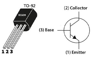
The pin configuration of the BC639 Transistor is shown below. This transistor includes three pins which are discussed below.

BC639 Transistor Pin Configuration
- Pin-1 (Emitter): The flow of electrons will emit from the emitter to the primary PN junction
- Pin-2 (Collector): This pin collects the electrons that are emitted from the emitter of the transistor.
- Pin-3 (Base): The base terminal helps in controlling the transistor biasing.
Features & Specifications:
The features and specifications of the BC639 transistor include the following.
- BC639 is an NPN Bipolar and high-voltage transistor.
- It is available within the TO-92 package.
- The maximum DC current gain or hFE of this transistor is 160.
- Its continuous collector current or IC is 1A.
- Its emitter to base voltage or VBE is 5Volts.
- Its base current or IB maximum is 100mA.
- Its maximum collector-to-base voltage or Vcb is 50 V.
- Its collector dissipation is 1W.
- Its transition frequency is 100 MHz.
- Its collector capacitance is 20pF.
- Its operating junction temperature or Tj range from -55 to 150℃.
- Its collector-to-emitter and collector-to-base voltage is 80V
- Its power dissipation is 800mW.
- Its DC current gain ranges from 40 to 160hFE.
- Its o/p capacitance or Cob is 7pF.
- Its transition frequency or FT is 200MHz.
- The saturation voltage from the collector to the emitter is 0.5V.
- The junction to ambient thermal resistance value is 200℃/W.
- The value of input capacitance for this transistor is 50pF.
- BC639 NPN transistor complementary is BC640 PNP transistor.
BC639 NPN transistor’s replacement / equivalents :
BC537, 2N5551, BC538, 2N5550, 2N5833, 2SC4145, 2N5831, 2SC2036, 2N5832, BDB01D, 2N2405, 2N5830, MPSL01, 2N2222, 2N4410, 2N4401, ECG123AP, BC337, etc. A transistor can be replaced with its equivalent in a circuit based on requirement. To know how to replace it, please refer to this; Replacing Transistors in Electronic Circuits: Factors and Considerations.
How to use BC639 Transistor Securely within a Circuit?
To use the BC639 transistor very securely within a circuit for a long time and also to get stable performance, stay 20% always under the highest ratings. Do not drive any load above 500mA & 80V DC. An appropriate base resistor always has to be used for providing the necessary base current and should not give a current above 100mA to the transistor’s base terminal. Store & use this type of transistor in the range of temperature > -65 centigrade & < +150 centigrade. To know how to choose the base resistance check on this link.
LED Driver Circuit using BC639 Transistor
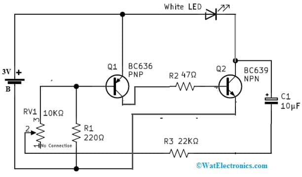
The circuit diagram of the LED driver using a BC639 transistor is shown below. This circuit is helpful to drive LED and control its brightness. This circuit provides PWM o/p through two transistors, a capacitor, and a timing resistor. In this circuit, 1 1-watt white LED is used as a target load. We know that the PWM technique is used mainly for controlling LED brightness as well as other devices that can be controlled quickly. The PWM technique controls the normally supplied voltage or current to the LED by regulating the on-off cycle of the duty cycle. Here both the Q1 and Q2 transistors through the RV1 timing Resistor & C1 timing capacitor will generate a PWM signal.
The required components to make this circuit mainly include; 3V battery, Q1 – BC636 PNP transistor, Q2 – BC639 NPN transistor, white LED, resistors R1 – 220Ω, R2 – 47Ω and R3-22KΩ, 10µF C1 capacitor and 10KΩ RV1 variable resistor. Connect the circuit as per the circuit shown below.

LED Driver Circuit using BC639 Transistor
Working
The working of this circuit follows as; the collector terminal of the Q1 transistor is connected simply to the base terminal of the Q2 Transistor. Here, Timing elements like R3, RV1, and C1 are connected in between the collector terminal of Q2 & base terminal of Q1. In this circuit, the light-emitting diode is connected between the +ve supply & collector terminal of Q2.
Once the battery is connected to this simple circuit, capacitor C1 will get charged & discharge this cycle speed based on the variable resistor value. Based on the percentage of duty cycle, the LED in the circuit will glow. If the duty cycle of the PWM signal is 75%, then the LED will blink brighter as compared to the 50% duty cycle. Similarly, if the duty cycle of the PWM signal is 25% then the LED will blink dimmer.
The transistor can also be interfaced with a microcontroller for different applications. Read on transistor interfacing to microcontroller. A few precautions must be taken while connecting a transistor to the microcontroller. Click on the link to know more about it: Precautions to be taken before connecting a transistor to the microcontroller
Above all before using any of the transistors first we need to know how to choose a transistor for a circuit. Click this link How to Select a Transistor to know about it.
Applications
The applications of BC639 Transistor include the following.
- BC639 transistor is used within any general-purpose amplification & switching applications.
- This transistor has high collector current abilities to drive high-current relays, high-power LEDs, DC motors, high-power transistors, etc.
- This transistor is used at the o/p of microcontrollers & other types of electronic platforms such as Raspberry Pi and Arduino to drive loads.
- These transistors’ transition frequency is 200MHz so, it is used within RF circuits to perform well below 200MHz.
- These are used in sensor circuits, audio amplifier circuits, lighting systems, audio amplifier stages, relay drivers, signal amplifiers, RF circuits, simple switching, microphone preamplifiers, switching loads below 500mA – 1000mA, Darlington pairs, etc.
- These are used in the H-bridge, current mirror circuits, and for pre-amplification stages within different electronic circuits.
- These transistors are used in linear amplifiers, impedance buffering, oscillators & comparator-based circuits.
- These are used in astable multivibrator and bistable multivibrator-based circuits.
Please refer to this link for the BC639 Transistor Datasheet.
Thus, this is an overview of the BC639 transistor, pin configuration, specifications, circuit, working, and its applications. This is an NPN, high current gain BJT that carries low collector-emitter saturation voltage & high collector current, so it is extensively used for switching & amplification purposes. Here is a question for you, what is a BC636 transistor?