FET stands for the Field-effect transistor. These transistors are designed to overcome the drawbacks of the bipolar junction transistors. As the basic transistors have the junction of the emitter in the mode of forwarding bias this makes the device to operate at low impedance levels. This introduces considerable amounts of noise levels. FETs possess all the characteristics which can overcome the drawbacks of bipolar junction transistors and can be a good replacement for the vacuum tubes as well as BJTs. It also consists of three terminals. But these terminals are referred to as the source, drain, and gate.
These FETs are known for their unipolar characteristics. The reason behind its characteristics is that the functioning of this transistor depends upon the concentration of either holes or electron carriers. Field effect transistors can also be used in switching circuits, buffer amplification circuits and in integrated circuits.
What is a FET?
The transistor that is capable of transferring the signals from the high resistance to the low resistance values same like bipolar junction transistors but by overcoming the disadvantages of it in its uni-polar way is defined as a field-effect transistor (FET).
FET is designed in such a way there exist three terminals that are known as source, gate and the drain. These terminals are responsible for the influencing of the majority carriers by supplying it with possible supplies of voltages. This leads to the generation of the current. The flow of current can be controlled by the applying the voltage justifying the characteristics that it is a voltage-controlled device.
Types of FET
Based on its construction FET’s are classified as
(1) Junction Field Effect Transistor (JFET)
These JFET’s working is based on the channels formed between the terminals. The channel can be of either n-type or the p-type. Because of the n-type channel, it is referred to as n- channel JFET and due to a p-type channel formed it is referred to as p-channel JFET.

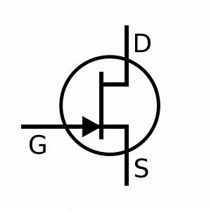
Symbol of N-Channel JFET
JFET Working
The construction of the JFET is as similar to that of BJT it can be formed by using n-type and p-type materials. N-type is placed in between p-types or the p-types is placed in between n-types. As like N-P-N and P-N-P transistors formed in BJT, these are also formed in FET. These JFET’s consists of the channel that may be n or p-type.

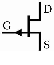
Symbol for P-Channel JFET
- Based on the channel it is known as n-channel JFET or the p-channel JFET.
- For the n-channel JFET, the positive side is connected to the source terminal.
- The drain terminal receives the highest potential in comparison with the gate in this n-channel JFET.
- The junction formed due to the interaction of the drain and the gate terminal will be in reverse bias.
- Due to this reason, the width of the depletion region that is present near to the drain is greater in comparison with the source.
- Because of this condition, the majority of the charge carriers that are electrons flow can be seen from the terminals drain to the source.
- As this potential at drain tends to increase the flow of carriers increases the flow of current also increases.
- But certain increment at the voltages at drain and source the flow of current is stopped.
- The JFET is generally known for the characteristics of controlling the current by the application of the input voltages.
- The value of the input impedance is at a peak in this transistor.
- When the JFET is in its ideal mode there is no current evidence at the gate terminal.
That how a n-channel JFET works. Only the variation at the polarities of the supplies makes the FET work as p-channel JFET.
(2) Metal Oxide Semiconductor Field Effect Transistor (MOSFET)
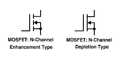
In MOSFETs, the functioning is based on the channels which already exist or formed when a voltage is applied. Based on these modes of operations MOSFETs are further classified into Depletion mode and the enhancement mode. In the enhanacement mode the channel is induced due to the application of the voltage at the gate but in the depletion mode, the MOSFET is operated due to the already existing channel in it.

MOSFET
MOSFET Types:
The depletion model of MOSFET is also classified into ntype and ptype. The only difference between this is the deposition of the substrates. Due to the concentration of the carriers that are preferably the majority is responsible for the formation of the region called depletion. This width of the depletion is responsible for the effect of conductivity.
In the enhancement mode when a voltage applied to the gate terminal beyound a threshold voltage a channel is formed. It may be n-type for P type susbstrate and p- type for an N type substate. Based on the channel formation enhancement mode is classified as N type Enhancement MOSFET and P type Enhancement MOSFET. Enhancement type MOSFET are most widely used than the depletion type.
Biasing
The FET biasing is also done like transistor biasing. It can be fixed bias, self-bias, and the potential- Divider biasing.
(1) Fixed Bias
Fixed bias in the FET can be obtained by supplying with the battery voltage. The terminal gate must connect with the negative supply of the battery and no current flow is evident through the resistor.
(2) Self Bias
As the name suggests if the external supply is not provided for the circuitry. This type of bias is known as self-bias. Any changes in the transconductance values that reflect the distortion of the operating point. These parameters can be controlled and they are not easily affected in the self-bias.
(3) Potential Divider Bias
The circuit is provided with the supply at the input but the two resistors are connected in such a way that the voltage at the input is divided with the help of resistors. Hence this circuitry is referred to as potential divider.
These biasing techniques are chosen based on the necessity and the increment of the conductance values.
Characteristics
The FET characteristics mainly depend on the various operating regions. The regions are ohmic, saturation, cut-off and the breakdown region.
(1) Ohmic Region
The region at which the transconductance shows the linear response and the current at the terminal gate is opposed by the resistance is known as ohmic region.
(2) Saturation Region
At this region, the device is at fully ON mode. During this condition the maximum amount of current flow through the transistor at a steady state.
(3) Cut- off Region
There is no flow of current can be evident at the transistor during this region. Hence it is referred to as the device in the OFF condition.
(4) Breakdown Region
When the applied voltage exceeds the condition of the maximum value of the voltage then the transistor enters into the breakdown condition indicating that the transistor resists the flow of current.
Applications
The applications of the FET are as follows
- For applications like low noise, these types of transistors are preferred.
- FET’s have a preferred utilization during the applications of it as a buffer.
- These are used in the cascade amplifiers.
- The main feature behind this is that its input capacitance is low.
- For analog switching, the FET is preferred.
- It is preferred during oscillation circuits.
- For the current limiting circuits JFET’s are preferred.
In this way, the field-effect transistors have many applications. It may be JFET or the MOSFET both have many applications based on its highly unified characteristics. Each of it is preferred as switches and can be used in amplifications etc…
FET as a Switch
FET can be used as one of the applications of switching because it can be operated as either fully ON and the fully OFF. Similar to BJTs a FET also consists of the active region, cut-off region, and the saturation region as mentioned above.
As the voltage applied at the junction of gate and source is zero then the working condition of FET is in saturation because the maximum amount of the current flows through it. When the applied voltage that is lesser than the cut-in voltage or more negative.
Then the operating region of the FET is considered to be in cut-off mode. During its working in the cut-off region, there is no evident flow of the current through the circuit. These are the reasons due to which the FET operates as a switch. When the FET is connected with the load in a parallel manner then it acts as an analog switch. FET’s can also be connected in the series to act as a series switch.
In this way, the basic operation of the FET along with its types and the biasing techniques have been discussed above. The junction field-effect transistor is the first classification of the FET that is classified based on the junctions formed of –type or p-type. These FETs classification based on the channels formed are done known as MOSFETs.
Please refer to this for How to Select a Transistor.
Please refer to this link for Field-Effect Transistors MCQs
After analyzing the types of FETs can you describe which one is better and mostly the preferable one among JFET and MOSFET?