ARM Processor
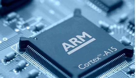
The ARM microcontroller stands for Advance RISC Machine; it is one of the extensive and most licensed processor cores in the world. The first ARM processor was developed in the year 1978 by Cambridge University, and the first ARM RISC processor was produced by the Acorn Group of Computers in the year 1985. These processors are specifically used in portable devices like digital cameras, mobile phones, home networking modules and wireless communication technologies and other embedded systems due to the benefits, such as low power consumption, reasonable performance, etc. This article gives an overview of ARM architecture with each module’s principle of working.
ARM Architecture
The ARM architecture processor is an advanced reduced instruction set computing [RISC] machine and it’s a 32bit reduced instruction set computer (RISC) microcontroller. It was introduced by the Acron computer organization in 1987. This ARM is a family of microcontroller developed by makers like ST Microelectronics,Motorola, and so on. The ARM architecture comes with totally different versions like ARMv1, ARMv2, etc., and, each one has its own advantage and disadvantages.
ARM Architecture
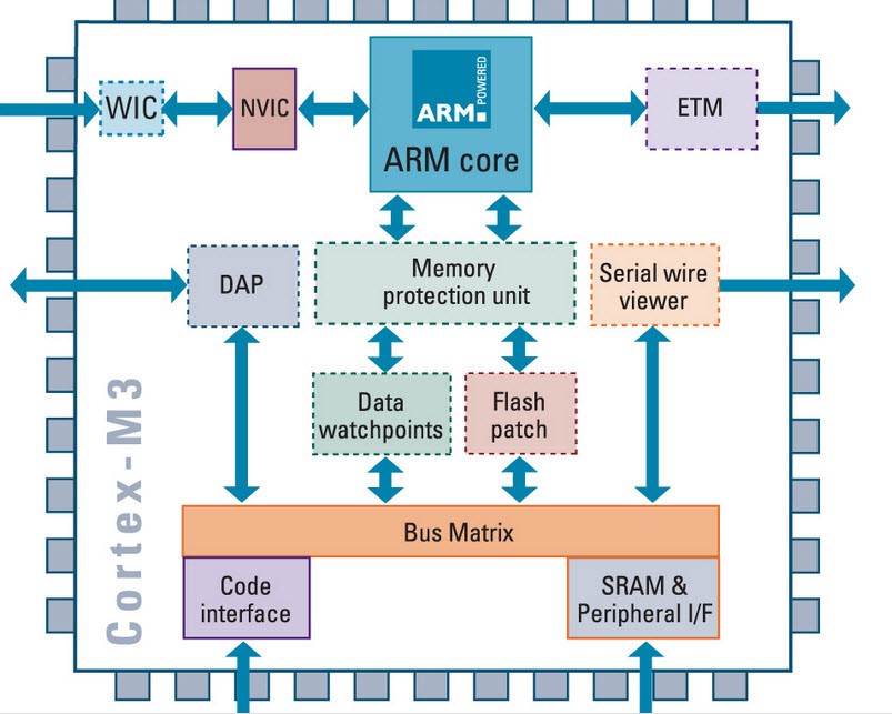
The ARM cortex is a complicated microcontroller within the ARM family that has ARMv7 design. There are 3 subfamilies within the ARM cortex family :
- ARM Cortex Ax-series
- ARM-Cortex Rx-series
- ARM-Cortex Mx-series
The ARM Architecture
- Arithmetic Logic Unit
- Booth multiplier
- Barrel shifter
- Control unit
- Register file
This article covers the below mentioned components.
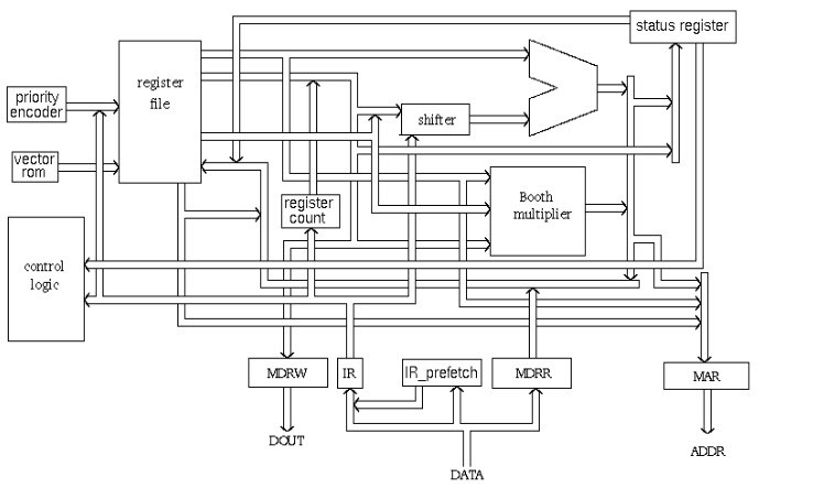
The ARM processor conjointly has other components like the Program status register, which contains the processor flags (Z, S, V and C). The modes bits conjointly exist within the program standing register, in addition to the interrupt and quick interrupt disable bits; Some special registers: Some registers are used like the instruction, memory data read and write registers and memory address register.
Priority encoder: The encoder is used in the multiple load and store instruction to point which register within the register file to be loaded or kept .
Multiplexers: several multiplexers are accustomed to the management operation of the processor buses. Because of the restricted project time, we tend to implement these components in a very behavioral model. Each component is described with an entity. Every entity has its own architecture, which can be optimized for certain necessities depending on its application. This creates the design easier to construct and maintain.
ARM Block Diagram
Arithmetic Logic Unit (ALU)
The ALU has two 32-bits inputs. The primary comes from the register file, whereas the other comes from the shifter. Status registers flags modified by the ALU outputs. The V-bit output goes to the V flag as well as the Count goes to the C flag. Whereas the foremost significant bit really represents the S flag, the ALU output operation is done by NORed to get the Z flag. The ALU has a 4-bit function bus that permits up to 16 opcode to be implemented.
Booth Multiplier Factor
The multiplier factor has 3 32-bit inputs and the inputs return from the register file. The multiplier output is barely 32-Least Significant Bits of the merchandise. The entity representation of the multiplier factor is shown in the above block diagram. The multiplication starts whenever the beginning 04 input goes active. Fin of the output goes high when finishing.
Booth Algorithm
Booth algorithm is a noteworthy multiplication algorithmic rule for 2’s complement numbers. This treats positive and negative numbers uniformly. Moreover, the runs of 0’s or 1’s within the multiplier factor are skipped over without any addition or subtraction being performed, thereby creating possible quicker multiplication. The figure shows the simulation results for the multiplier test bench. It’s clear that the multiplication finishes only in16 clock cycle.
Barrel Shifter
The barrel shifter features a 32-bit input to be shifted. This input is coming back from the register file or it might be immediate data. The shifter has different control inputs coming back from the instruction register. The Shift field within the instruction controls the operation of the barrel shifter. This field indicates the kind of shift to be performed (logical left or right, arithmetic right or rotate right). The quantity by which the register ought to be shifted is contained in an immediate field within the instruction or it might be the lower 6 bits of a register within the register file.
The shift_val input bus is 6-bits, permitting up to 32 bit shift. The shifttype indicates the needed shift sort of 00, 01, 10, 11 are corresponding to shift left, shift right, an arithmetic shift right and rotate right, respectively. The barrel shifter is especially created with multiplexers.
Control Unit
For any microprocessor, control unit is the heart of the whole process and it is responsible for the system operation,so the control unit design is the most important part within the whole design. The control unit is sometimes a pure combinational circuit design. Here, the control unit is implemented by easy state machine. The processor timing is additionally included within the control unit. Signals from the control unit are connected to each component within the processor to supervise its operation.
Please refer to this link to know more about ARM MCQs
ARM7 Functional Diagram
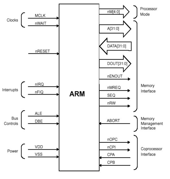
The final thing that must be explained is how the ARM will be used and the way in which the chip appear. The various signals that interface with the processor are input, output or supervisory signals which will be used to control the ARM operation.
ARM Functional Diagram
ARM Microcontroller Register Modes
An ARM micrcontroller is a load store reducing instruction set computer architecture means the core cannot directly operate with the memory. The data operations must be done by the registers and the information is stored in the memory by an address. The ARM cortex-M3 consists of 37 register sets wherein 31 are general purpose registers and 6 are status registers. The ARM uses seven processing modes to run the user task.
- USER Mode
- FIQ Mode
- IRQ Mode
- SVC Mode
- UNDEFINED Mode
- ABORT Mode
- Monitor Mode
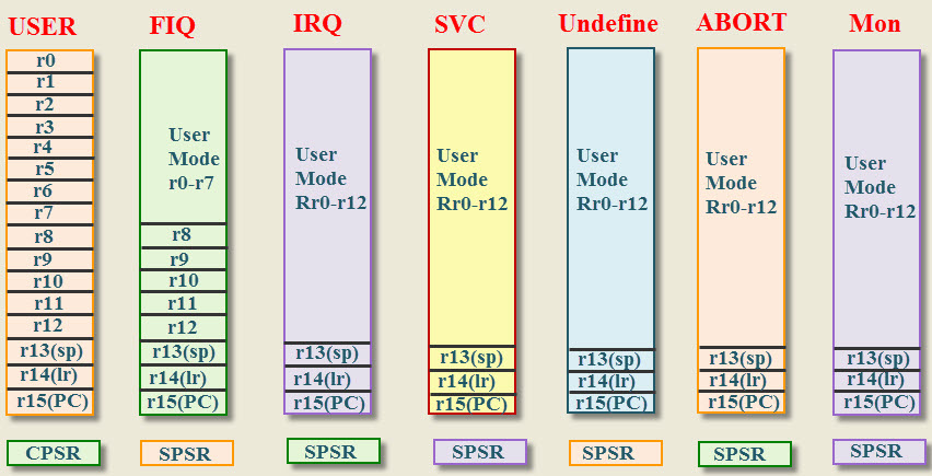
ARM Microcontroller Register Modes
USER Mode: The user mode is a normal mode, which has the least number of registers. It doesn’t have SPSR and has limited access to the CPSR.
FIQ and IRQ: The FIQ and IRQ are the two interrupt caused modes of the CPU. The FIQ is processing interrupt and IRQ is standard interrupt. The FIQ mode has additional five banked registers to provide more flexibility and high performance when critical interrupts are handled.
SVC Mode: The Supervisor mode is the software interrupt mode of the processor to start up or reset.
Undefined Mode: The Undefined mode traps when illegal instructions are executed. The ARM core consists of 32-bit data bus and faster data flow.
THUMB Mode: In THUMB mode 32-bit data is divided into 16-bits and increases the processing speed.
THUMB-2 Mode: In THUMB-2 mode the instructions can be either 16-bit or 32-bit and it increases the performance of the ARM cortex –M3 microcontroller. The ARM cortex-m3 microcontroller uses only THUMB-2 instructions.
Some of the registers are reserved in each mode for the specific use of the core. The reserved registers are
- Stack Pointer (SP).
- Link Register (LR).
- Program Counter (PC).
- Current Program Status Register (CPSR).
- Saved Program Status Register (SPSR).
The reserved registers are used for specific functions. The SPSR and CPSR contain the status control bits which are used to store the temporary data. The SPSR and CPSR register have some properties that are defined operating modes, Interrupt enable or disable flags and ALU status flag. The ARM core operates in two states 32-bit state or THUMBS state.
ARM-Cortex Microcontroller Programming
In the present days, the microcontroller vendors are offering 32-bit microcontrollers based on ARM cortex-m3 architecture. Many embedded system developers are starting to use these 32-bit microcontrollers for their projects. The ARM microcontrollers supports for both low-level and high level programming languages. Some of the traditional microcontroller architectures are made with many limitations therefore, difficult to use the high level programming language.
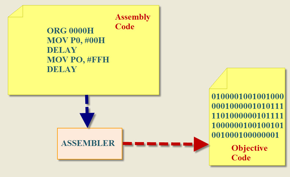
ARM-Cortex Microcontroller Programming
For example the memory size is limited and performance might not be sufficient. The ARM microcontrollers runs at 100Mhz frequency and higher performance, therefore it supports the higher level languages. The ARM microcontroller is programmed with different IDES such as keiluvision3, keiluvision4, coocox and so on. A 8-bit microcontroller use 8-bit instructions and the ARM cortex-M uses a 32-instructions.
Additional Uses of the Cortex Processor
It is a reduced instruction set computing Controller
- 32-bit high performance central processing unit
- 3-stage pipeline and compact one
It has THUMB-2 technology
- Merges optimally with 16/32 bit instructions
- High performance
It supports tools and RTOS and its core Sight debug and trace
- JTAG or 2-pin serial wire debugs connection
- Support for multiple processors
Low power Modes
- It supports sleep modes
- Control the software package
- Multiple power domains
Nested vectored interrupt controller (NVIC)
- Low latency, low noise interrupts response
- No need for assembly programming
ARM Cortex (STM32) based Solar Street Light
Present days, solar technology has been progressing in many applications like homes, industries, etc. The main goal of this project is to conserve the electrical energy:here an Arm-Cortex- based solar street light is implemented that works on solar energy. Generally, solar street lights are used where electricity is not available.
Hardware Components
- STM32 with ARM cortex board
- White LEDs
- MOSFET
- Battery
- Regulator
- Solar Panel
Software
- Keil compiler
- Embedded C Language
This project utilizes an ARM-Cortex processor of the STM32 family and a battery for power supply. This project uses a solar panel to charge the battery where charge controller circuit controls the battery charging. ARM-Cortex processor is interfaced to a set of LEDs with the help of the MOSFET Switch.
The intensity control of the LED lights is possible by varying the duty cycle from a DC source. A programmed ARM-Cortex microcontroller unit is engaged to afford different intensities at different times of night by using the Pulse Width Modulation technique. The charge controller circuit is used to protect the battery from the deep discharge and overload conditions.
The ARM Microcontroller Assembly Level Programming:
The ARM cortex microcontroller is a 32-bit microcontroller therefore all instructions are 32-bit long which is executed in a single cycle. It consists of an instruction set to perform the arithmetic, logical and boolean operations. The ARM is a load-store architecture, then instructions are executed conditionally.
Syntax: Load a // a obtained the value from the place called a //
ADD12 // 12 is added to the load value a //
Store a // final value is stored in the variable a//
The assembly language programming is developed by the mnemonics such as ADD, SUB, MUL so on but for ARM programming, some extra instructions added such as ADCNES and SWINE, etc.
EX: 1. ORG 0000h
MOV r1, #10
MOV r2, #15
ADD r3, r2, r1 // r3=r2+r1 and the final value stored in r3 register//
2.ORG 0000h
MOV r1, #10
MOV r2, #15
SUB r3, r2, r1 // r3=r2-r1 and the final value stored in r3 register//
The ARM Coretex-M3 Microcontroller Embedded C Level Programming:
WAP to toggle the single LED through Embedded C language using ARM cortex microcontroller.
#include “stm32f10x_gpio.h”
#include “stm32f10x_rcc.h”
GPIO_InitTypeDef GPIO_InitStructure;
int i;
#define LED_PORT GPIOB
Void binky();
Void main()
{
Void binky();
}
void binky(void)
{
RCC_APB2PeriphClockCmd(RCC_APB2Periph_GPIOB, ENABLE); //enable the PORTB pins//
GPIO_InitStructure.GPIO_Speed = GPIO_Speed_50MHz; //set the port frequency//
GPIO_InitStructure.GPIO_Mode = GPIO_Mode_Out_PP; //set the PORTB in output//
GPIO_InitStructure.GPIO_Pin = GPIO_Pin_All ; //enabled all PORTB pins//
GPIO_Init(GPIOB, &GPIO_InitStructure); //initialize the PORTB pins//
while(1){
GPIO_WriteBit(LED_PORT,GPIO_Pin_8,Bit_SET);
for (i=0;i<1000000;i++);
GPIO_WriteBit(LED_PORT,GPIO_Pin_8,Bit_RESET);
for (i=0;i<1000000;i++);
GPIO_WriteBit(LED_PORT,GPIO_Pin_9,Bit_SET);
for (i=0;i<1000000;i++);
GPIO_WriteBit(LED_PORT,GPIO_Pin_9,Bit_RESET);
for (i=0;i<1000000;i++);
GPIO_WriteBit(LED_PORT,GPIO_Pin_10,Bit_SET);
for (i=0;i<1000000;i++);
GPIO_WriteBit(LED_PORT,GPIO_Pin_10,Bit_RESET);
for (i=0;i<1000000;i++);
}
}
Please refer to this link to know more about ARM architecture Question & Answers.
Therefore, This is all about ARM architecture with an application. Furthermore, any queries regarding this article, You can write to us for developing and programming these projects practically and for some more latest arm processor based projects.
Photo Credits:
- ARM Block Diagram by sourceforge