In the domain of digital electronics logic gates are the devices that perform Boolean operations having two inputs and one output. Depending on the logical gate, the logical functionality changes and the output also gets varied. In the year 1886, in a letter, Charles Pierce stated that how logical functionalities could be performed by switching circuits. Finally, vacuum tubes got replaced by logical operations. And the one logical gate which we are going to discuss today is AND gate. The first and modern AND gate was invented by Walther Bothe in the year 1954. This article explains how to define AND gate, its circuit, its development using transistor, multiplexer, and applications.
What is AND Gate?
This gate is a logic gate that accepts either two/more inputs and shows the result as a single output. When both the inputs are at logic ‘0’, then the output is also logic ‘0’ (LOW) and when both the inputs are at logic ‘1’, then the output is also logic ‘1’ (HIGH). The functionality is the same even the gate has either 2-inputs, 3-inputs, and more. The AND gate rules are based on the operation of logical multiplication.
AND Gate Theory
To have a clear understanding, let us know how it performs corresponding to its inputs.
Consider there are two binary inputs, ‘0’ and ‘1’. As the operation is based on binary multiplication. So, when ‘0’ is multiplied by ‘1’, or ‘1’ is multiplied by ‘0’ the output is ‘0’. The output is ‘1’ only when ‘1’is multiplied by ‘1’. That is
0 × 0 = 0
0 × 1 = 0
1 × 0 = 0
1 × 1 = 1
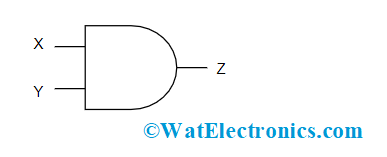
The symbol is shown below:
Basic AND Gate
Here, X and Y are considered as inputs and Z is the output. The X and Y inputs can be either ‘0’ or ‘1’.
It may have multiple inputs but has only one output. With this, the logical formula is given as
XY = Z
All the combinations of X and Y are represented in a tabular format which is the AND gate truth table and it is shown below. The truth table shows the result of corresponding digital logic for all the possible input combinations. Here,
| X | Y | Z |
| 0 | 0 | 0 |
| 0 | 1 | 0 |
| 1 | 0 | 0 |
| 1 | 1 | 1 |
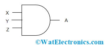
The above truth table is for 2-input AND gate. For example, the below picture shows the AND gate structure when it has three inputs then the logical representation and truth table are represented as follows:
XYZ = A
The logical diagram is
3 Input AND Gate
The truth table when the gate has three inputs, and one output is:
| X | Y | Z | A |
| 0 | 0 | 0 | 0 |
| 0 | 0 | 1 | 0 |
| 0 | 1 | 0 | 0 |
| 0 | 1 | 1 | 0 |
| 1 | 0 | 0 | 0 |
| 1 | 0 | 1 | 0 |
| 1 | 1 | 0 | 0 |
| 1 | 1 | 1 | 1 |
Multi-input AND gate
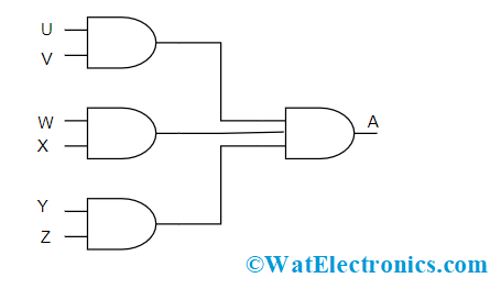
The below picture shows how an the gate is constructed with multiple input bits.
Consider we have 6 inputs as U, V, W, X, Y, and Z. Then the output is
Multi Input Gate
A = (U.V). (W.X). (Y.Z)
When the total number of inputs is odd and if any of the inputs are unused then they can be at HIGH by connecting them to the power supply through pull-up resistors.
Operation using Diode
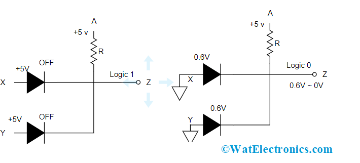
In general, the AND operation is performed either by diodes or transistors. When the gate is designed using diodes, it is termed as diode AND gate. And the AND gate circuit diagram using diode is:
AND Gate Using Diode
As per the above circuit, initially, a 5V level of voltage is applied at point A, then +5V is given at points X and Y. Now, both the diodes will be in reverse biased condition and move to OFF condition. In this condition, the circuit performs as an open circuit where there will be no current flow across the resistor and +5V flows till the output pin ‘Z’. As the output has a certain voltage, the result is considered as logic ‘HIGH’.
Whereas when either of the input pins is applied with 0V or when they are grounded, then the diodes will be in forward biased state, and the circuit moves to ON condition. Now, the supply voltage applied at point A will get a path through any of the diodes or both of them to the ground. As the current flow is from point A to ground via R resistor, then the entire supply voltage gets dropped at the resistor and so there will be no output at point Z and the result is considered as logic ‘LOW’.
When the diodes are in forward bias, then there will be some level of voltage drop and this equals to forward bias voltage level. The corresponding voltage drop appears at ‘Z’ which means that the voltage at the output pin is 0.6 Volts or 0.7 Volts which is nearly considered as ‘0’. This is the operation of AND gate using diode.
AND Gate using Transistor
The operation and construction of an AND functionality can also be derived using a transistor. Below is the circuit diagram using a transistor.
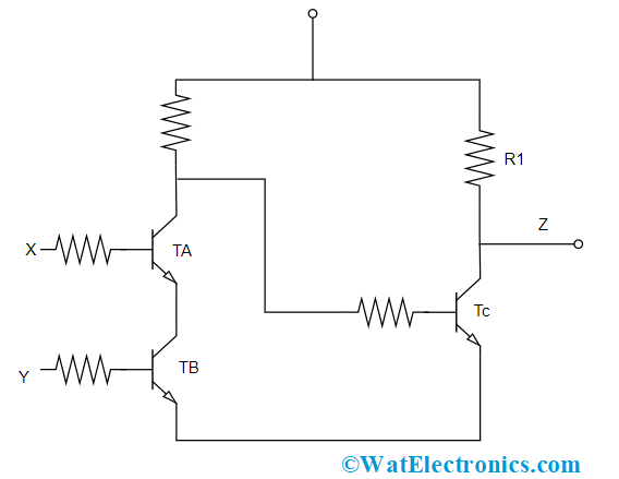
Transistor Circuit of AND
Case 1:
When the input pins X and Y are provided with ‘0’ Volts or when both the pins are grounded, then the transistors TA and TB move into OFF condition correspondingly. Because the input pins are connected to the base terminals of both the transistors so that transistor will be in an OFF state for zero base voltage level. When the path across TA and TB becomes open-circuit, then TC transistor base gets the required amount of potential so that it will be in ON state.
At this condition, current starts to flow from supply to ground via TC transistor. Then, the entire supply voltage drops down at resistor R1, making the output voltage level at terminal Z ‘0’. This is the same condition when either of the transistors TA and TB is in OFF condition as those are connected in series.
Case 2:
When both the input pins X and Y are applied with high logic (+5V) which means the base terminals of both the transistors have +5V voltage. This makes the transistors TA and TB in ON state. With this, the entire supply voltage drops down at resistor R1 and the Tc transistor base will have 0 volts so that it moves into OFF condition. On the whole, the supply voltage appears at output pin Z which means the result is logic HIGH.
This is the working scenario using transistors.
AND gate using Multiplexer
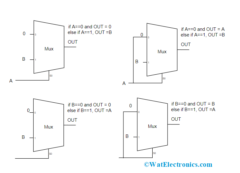
When the truth table is observed, it is seen that when either of the inputs is at logic LOW, then the output is LOW and when both the inputs are at logic HIGH, then the output is HIGH. This corresponds that the result is based on both of the inputs. With this, the AND operation using a multiplexer can be represented in four ways as shown in the below picture.
MUX Using AND
The truth table is:
| A | B | S0 | S0 – > B |
| 0 | 0 | 0 | S0 = 0 |
| 0 | 1 | 0 | |
| 1 | 0 | 0 | S0 = B |
| 1 | 1 | 1 |
So, an AND operation using MUX can be derived by ‘n-1’ selection lines.
AND Gate implementation using NOR Gate
To implement an AND operation using the NOR gate, it is suggested to know about DeMorgan’s theorem. This theorem states that the sum of the complement of inputs is equal to the complement of the product of the inputs. This can be represented as:
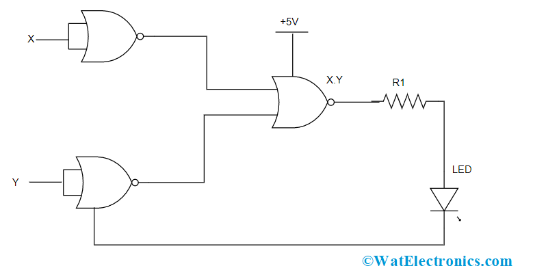
AND Gate using NOR
(X+Y)’ = X’ . Y’
As per the above circuit, two NOR gates are used where the input terminals of both gates are shorted. This gives the output as X’ + Y’
Then this output is provided as input to other NOR gates where this provides the result as (X’ + Y’)’
- (X’)’ + (B’)’
- Y
So, the result is the product of two inputs which is
X.Y
ICs of AND gate
IC 7408
In TTL logic, the IC of AND gate is 7408. This is a Quad 2-input IC that consists of four gates. The pin diagram of the IC is shown below:
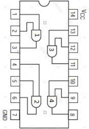
IC 7408
As there are four gates, pins 1 and 2 are the inputs of gate 1 and its corresponding output is at pin 3. In the same way, for gate 2, the inputs are at pins 4 and 5 and its corresponding output is at pin 6. For the fourth gate, the inputs are at pins 12 and 13 and the output is at pin 11.
The 14th pin provides the supply voltage to the IC and the maximum level of voltage provided to the IC is 5.2 volts and above this level of voltage causes loss to the IC.
IC 4081
In CMOS logic, the IC of AND gate is 4081. This is a Quad 2-input IC that consists of four gates. The pin diagram of the IC is shown below:
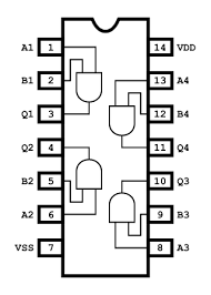
IC 4081
As there are four gates, pins 1 and 2 are the inputs of gate 1 and its corresponding output is at pin 3. In the same way, for gate 2, the inputs are at pins 5 and 6 and its corresponding output is at pin 4. For the third gate, the inputs are at pins 8 and 9 and the output is at pin 10. Pin 7 is grounded.
And for the fourth gate, the inputs are present at pins 12 and 13 and the output is at pin 11. The 14th pin provides a supply voltage to the IC with a maximum level of 5.2 volts. Here, a direct current can be provided where it activates the IC. Here also, providing a high level of voltage causes damage to the IC.
The other ICs are:
74LS11 – 3 input TTL AND Gate
This IC consists of three independent gates where every gate performs AND operation.
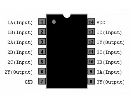
74LS11
The functional conditions of 74LS11 are:
- Supply voltage – minimum of 4.75 Volts and maximum of 5.25 volts
- LOW and HIGH-level input voltages are 0.8V and 2V
- HIGH and LOW-level output currents are 8 Amps and -0.4 Amps
- Its free air functional temperature lies in the range of 0 to 700C
- The switching characteristics of 74LS 11 are:
- The propagation delay in time from LOW to HIGH level lies in the range of 4 – 13 ns for a CL of 15pF and 6 – 18 ns for a CL of 50 pF
- The propagation delay in time from HIGH to LOW level lies in the range of 3 – 11 ns for a CL of 15pF and 5 – 18 ns for a CL of 50 pF
CD4073 – 3 input CMOS
This gate is designed by CMOS technology which is combined both with the N and P-type of MOSFET devices. Using this IC, system manufacturers use the operation of the AND gate and complement the prevailing group of CMOS gates.
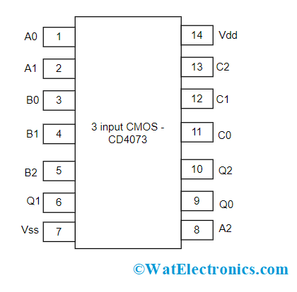
CD4073
The advantage of this IC is that it performs across a wide range of voltages so that it can be utilized in various DLD designs. The output of CD4073 is present in TTL logic which allows the device to easy interface with NMOS, CMOS, and TTL circuits. This is a 14-pin IC and its pinout structure is explained as follows:
- A0, A1, and A2 are the input pins of Gate 1
- B0, B1, and B2 are the input pins of Gate 2
- C0, C1, and C2 are the input pins of Gate 3
- Vss and Vdd are the source and drain supplies of IC
- Q0, Q1 and Q2 are the output pins of gate 1, gate 2, and gate 3
The key characteristics of CD4073 IC are:
- The operational speed is 60 ns at a supply voltage of 10V
- The maximum level of the input current is 1µA at a voltage level of 18V having a temperature range of 100nAmps
Applications
- The main AND gate application is in digital electronics and in data transmission. Where AND gate helps for allowing or not allowing the data through a channel.
- Used in digital measuring devices
- Used in alarm circuits
- The other application is Inhibit gate. This is the reverse approach of enabling gate
- Automatic temperature-regulating circuits
- Freezer warning buzzer devices
Please refer to this link to know more about Open Drain and Freewheeling Diode.
This is all about the concept of logic AND gate. This article has provided a detailed explanation of how an AND gate performs, its circuit diagram, truth table, AND gate ICs, examples, and applications. Also, know how the gate performs AND gate multiplication and AND gate division?