In 1963, Sylvania as Sylvania Universal High-Level Logic (SUHL) introduced the first Transistor-Transistor Logic circuits. The concept of TTL was developed to achieve high speed, low power dissipation that allows optimization of the design. It belongs to the digital logic family and is designed with bipolar transistors, resistors, and diodes. It is widely used in various applications such as electronic devices, computer control systems, industrial controlling systems, the design and fabrication of integrated circuits, and many more. This article gives a brief description of the internal structure and working of a transistor-transistor logic circuit with a 2-input NAND gate function.
What is Transistor-Transistor Logic Or TTL?
Transistor-transistor logic (TTL) is an integrated circuit that performs a logic function to provide a switching function by using bipolar transistors. The most important feature of the TTL device is that the inputs of the gate will be logic high (1) if they are not connected.
This technology is used to design and fabricate integrated chips, which contain logic gates and bipolar transistors, resistors, and diodes. It resolves the capacitive loading problem and speed problems that arose in DTL because transistors are used instead of diodes. It provides better noise rejection and excellent capacitive loading characteristics. It has 10ns of propagation delay and 10mW of power dissipation.
The circuit is designed with multiple emitters with multiple inputs. There are different logic families in TTL circuits. They are,
Standard TTL (74)
This is the first TTL IC developed in the year 1965 to perform basic logic functions. These are used as glue logic, which can connect more complex devices in digital systems. It is used in various applications in a combination with speed and dissipation.
Schottky TTL (74S)
It is another subfamily of TTLs. This is used to speed up execution. The speed offered by this type of TTL is twice that of high-power TTL. The power dissipation is the same for both TTLs and there is no additional power consumption. The circuit design is very similar to high-power TTL. The Schottky transistor used in this type of TTL is nothing more than a bipolar transistor, the base, and collector of which are connected by a Schottky diode. This TTL Schottky is further subdivided into many types such as Low Power Schottky, Low Power Schottky, and Extended Schottky TTLs.
High power TTL (74H)
The high power TTL is the high-speed version of standard TTL. The operating speed and power dissipation are higher than low-power TTL. The circuit is designed as a high-performance TTL NAND gate where NAND elements are four-pair inputs of type 74H00 or 54H00.
Low power TTL (74L)
It is another subfamily of TTL and is called a low-power TTL because of its low power consumption and power wastage. Although the speed of the operation performed is reduced. This TTL is generated by an AND gate. The NAND gates used here are type 74L00 or 54L00 and are of the 2-input and 4-input types. The construction is nearly identical to standard TTL, except for higher value resistors. For this increase in resistance, the power dissipated in the circuit is reduced.
Fast TTL (74F) and Advanced Schottky TTL (74AS)
These TTLs are the LS variants from Fairchild and TI, circa 1985, with “Miller-Killer” circuit designs to speed up the transition from low to high. These achieved PDPs of 10 pJ and 4 pJ, respectively, which are the lowest of all TTL families.
Advanced low power TTL (74ALS)
It is low voltage TTL (LVTT) for power supply applications of 3.3V and memory interfacing.
The TTL logic integrated chips are available in the 7400 series. Based on the logic families integration, the number of IC changes in the output will be either logic 1 or logic 0 based on the given supply voltage to the TTL. If the supply voltage is positive at 5 volts, then the output voltage will be 0V-0.4V for logic 0, and 2.4V-5V for logic 1.
How does a Transistor-Transistor Logic Circuit Work?
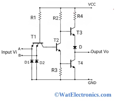
To understand the working of Transistor-Transistor logic (TTL), consider the circuit diagram of the standard TTL logic gate, which executes a positive NAND gate function as shown in the figure below. This standard TTL logic circuit is related to the Diode-Transistor Logic (DTL) circuit in some conditions.

TTL Circuit with 2-Input NAND Gate
From the above figure, T1 is the input transistor, which has an advantage in switching time. The transistor T2 is a phase-splitter and the transistors T3&T4 give totem-pole output. This TTL circuit has very low input impedance, high fan-out, and better noise immunity and is capable of a high capacitive drive.
When the inputs A and B are HIGH, the transistors T2 and T3 turn ON and act as common-emitter amplifiers. The transistor T4 and the diodes at the emitter are forward biased and a negligible amount of current flows. The output is LOW, which represents logic 0.
When both the inputs are LOW, diodes D1 and D2 get forward biased. The current goes to the ground via the D1&D2 and the resistor R1 due to the supply voltage VCC of 5V. The voltage supply drops in R1 and the transistor T2 turns OFF because it has not had enough voltage to turn ON. Therefore, the transistor T4 also turns OFF due to T2 being OFF. The transistor T3 turns ON (HIGH) and acts as an emitter follower. The output is HIGH, which represents logic 1.
When any one of the inputs A and B is low, then the diode gets forward biased due to the low input. The whole operation is the same as described above. Therefore, the output is HIGH (logic 1).
Transistor-Transistor Logic Operation Principle
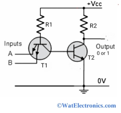
Transistor-Transistor Logic (TTL) is one of the digital circuits designed from BJT (Bipolar Junction Transistor) and resistors. The operation principle of TTL is based on the switching function of logic gates and amplification performed by the transistors in the circuit. To understand this, consider a basic transistor-Transistor logic circuit diagram as shown in the figure below.

TTL Simplified Circuit Diagram
The basic diode-resistor logic formed with AND gate uses separate diodes for the inputs. Therefore, a bipolar junction transistor uses 2 junction diodes, which represent either NPN Or PNP transistors. So, the TTL (transistor-transistor logic) is formed when the input diodes of the DTL (Diode-Transistor Logic) are replaced with a single NPN transistor with multiple emitter inputs as shown in the above circuit.
The above circuit shows a simplified Transistor-Transistor Logic which functions as v a 2-input NAND gate. Here, T1 with 2 input emitter terminals acts as an input transistor, and T2 acts as a single-stage NPN inverting switching transistor.
When one or both emitter inputs A and B of T1 are connected to the logic LOW level (0), T1’s base current flows via the base or emitter junction to GND (0V), T1 saturated and is followed by the collector terminal. This causes the base of T2 to be grounded (0V). Therefore, T2 will be in the “OFF” state and the output at Q will be HIGH.
When both inputs “A” and “B” are at a logic HIGH level (1), the input transistor T1 turns OFF and the primary switching transistor T2 turns HIGH, making the Q output LOW due to the switching function of the transistor. Several emitters on T1 are connected as inputs to create a NAND gate function.
Transistor-Transistor Logic OR gate with Open Collector Output:
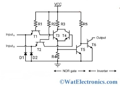
The circuit diagram of the transistor-Transistor logic 2-input OR gate with TTL NOR gate stage and open collector output stage (NOR gate output is connected to another transistor/inverter stage to make a TTL OR gate) is shown in the figure below. Transistors T1 and T2 are connected in the same way as seen for transistor T1 in other TTL circuits. Instead of working as an amplifier, T1 and T2 are used as a two-diode “drive” circuit. To illustrate the working, T1 and T2 can be replaced with a set of diodes.

TTL Circuit with OR Gate
From the above circuit diagram, the TTL logic NOR gate stage is converted into TTL logic OR gate by connecting the output logic level of the NOR gate to another transistor stage (inverter stage). That means the output stage of the TTL NOR gate is added to an inverter stage to create the TTL OR gate. Since totem-pole output stages are possible in both TTL circuits using 2-input OR gate and NOR gates.
When input A is connected to VCC, current flows through the base of transistor T3 and saturates. When input A is grounded, this current gets diverted from the base of T3 through the left control diode of T1, causing Q3 to turn OFF (cut-off). The same way is done for input B and transistor T4. The logic level at input B gives the conductivity of T4, which is either in saturation or cut-off.
Observe how transistors T3 and T4 are connected in parallel at the collector and emitter terminals. Essentially, these two transistors act as parallel switches, allowing current via resistors R3 & R4 depending on the logic level of inputs A & B.
When one of the inputs is HIGH (1), both/anyone transistors (T3 and/or T4) saturate, allowing the current through resistors R3 & R4 and reaches the logic output LOW level (0) on the TTL NOR gate output transistor T5. The output of the transistor T5 NOR gate circuit can only go high (1) when transistors T3 and T4 are OFF (cut-off). This means both inputs must be grounded or LOW (0) (TTL NOR gate condition to obtain output logic level HIGH) .
The output (logic 0) of the transistor T5 (TTL NOR gate output) obtained in the NOR gate stage is connected to transistor T6 (inverting output stage of NOR gate) to get the final output at the open collector output will be logic HIGH (1). This will be the output of the TTL OR gate when any one of the inputs A and B is HiGH (1).
Characteristics
The characteristics of TTL are a fan in and fan out, power dissipation, noise margin, and propagation delay.
Fan-in and Fan-out: The number of inputs and outputs connected to the gate that does not reduce voltage without affecting overall performance. Fan 10 for TTL.
Noise Margin: This is the allowable noise voltage at the input and should not affect the output. The noise margin of TTL is 0.4 V.
Propagation Delay: It refers to the time taken by the circuit from the application of input to the generated output.
Power Dissipation: This is the amount of power that the device requires. This is the product of the applied voltage and the current required to generate the output signal, measured in mW. Typically, TTL power dissipation is 10mW.
Advantages And Disadvantages
The advantages of transistor logic include the following.
- Less power dissipation when compared to RTL and DTL.
- Low cost.
- Good fan out and noise margin.
- Easy to interface several circuits
- It can generate complex logic functions.
- Can tolerate static electric discharges and avoids circuit damage.
- High reliability
- Faster
The disadvantages of transistor logic include the following.
- Not suitable for high-end electronic devices and processors which have high performance.
- Current consumption is high.
- In high current TTLs, the switching of output states can give improper functioning.
- Not used in complex logic circuits.
Applications
The transistor-transistor logic applications are given below.
- Microcontrollers and microprocessors.
- Light and remote controllers
- Controller circuits
- Processors in computer systems.
- Display driver circuits
- Small and low-power electronic devices.
Please refer to this for How to Select a Transistor.
Thus, this is all about an overview of Transistor-Transistor Logic (TTL). you can check your understanding by going through few basic questions at Transistor-Transistor Logic MCQs.TTLs are available in 74 series integrated circuits such as 74S86, 74ALS161, 7400, 7404, and 7402. Based on the application, check the specifications and choose the right TTL IC.