The initial invention of the class D amplifier took place in the year 1950 by Alec Reeves, but the device was actually called by the name class D in 1955. The first IC-based class D amplifier was introduced by Tripath in the year 1996 and this version was widespread across various domains. The need for class D amplifiers such as minimal power dissipation when compared with other topologies like class A, class AB and class B allowed class D to use in multiple applications. Also, minimal circuit spacing, cost, and enhanced battery life made us understand many of its concepts like class D amplifier definition, circuit, efficiency, working principle, and advantages.
What is Class D Amplifier?
Class D amplifier comes under the type of audio amplifier where the power management devices such as MOSFETs function as electronic switches. As these amplifying devices operate as perfect switching devices, no power and time will be wasted during the transition of phases in a zero input scenario. These amplifiers hold high power efficiency than their predecessor devices such as class AB, class B, and class A.
In the class D amplifiers, In the ON state, the binary switch passes the total current through it having no voltage across it. Whereas in the OFF state, it passes the total voltage through it having no current across it. This corresponds that the switches are in the condition of either completely ON or completely OFF thus showing decreased power losses in the output devices. This leads to class D amplifier efficiency of nearly 90 – 95%.
In the case of this switching device, the class D amplifier slew rate is known by the cut-off frequency of the output filter but not determined by the internal phases.
For example, An ideal square wave is passed via an inductance-capacitor filter. As the LC is a low pass filter, the passband range in this filter is limited and the bandwidth limitation has direct proportion with that of slew limitation.
The slew rate limitation of the circuit regulates the amount of maximum power delivered and distortion also and it is calculated in microseconds for every 1 volt of voltage. For a sine wave, the slew rate formula is given by
Slew Rate = (2 * π * frequency)/106 V/µsec
So with the above formula, slew rate can be known in microseconds that faultlessly reproduces the input supplied frequency having no distortion levels.
Block Diagram
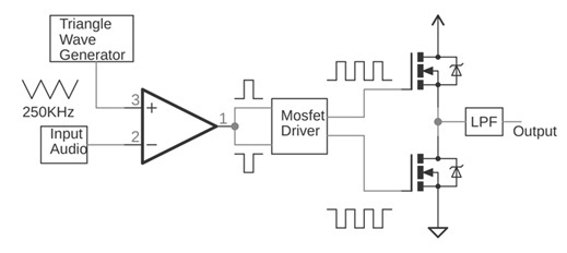
The class d amplifier block diagram is shown below. The class D amplifier is a switching amplifier because as compared to different amplifiers like class A, B, and AB, the class D amplifier can reach up to 90-95% of efficiency.

Class D Type Amplifier Block Diagram
The block diagram of a Class D amplifier mainly includes four different modules like a comparator, MOSFET driver, an LPF or low-pass filter, and a speaker. To understand the working of this amplifier, we have to learn how this amplifier works & how the switching signal is generated, For that, the following block diagram is explained.
In the above audio amplifier diagram, the audio input is given at the inverting terminal (-) of the comparator and a high-frequency triangular signal is given at the non-inverting terminal (+). Once the input audio signal’s voltage is higher than the triangular wave’s voltage then the comparator’s output goes high. Similarly, when the signal is low then the output of the comparator is low.
With this arrangement, the input audio signal is simply modulated through a high-frequency carrier signal, after that it connects to a MOSFET gate drive IC which drives the gate terminals of two MOSFETs for both the low side & high side once. At the output, we can get a powerful high-frequency square wave that passes through a low pass filter (LPF) stage to obtain our final audio signal.
Class D Amplifier using Tl494
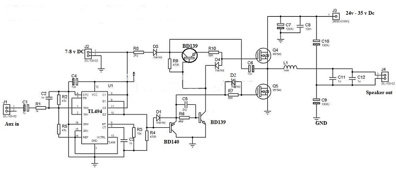
The other type which is most commonly used is the class D amplifier using Tl494 IC which is for pulse width modulation and includes an N-channel MOSFET transistor at the final stage of the amplifier. The amplifier using Tl494 has the input power supply in the range of 30V to 100V DC asymmetric power with the bias voltage of 8VDC to 12VDC. This type of configuration can deliver power of nearly 500 watts.
The Class D amplifier circuit using TL494 IC is shown below. This is a 500w high-efficiency amplifier circuit, so this amplifier can be used as a car sub amp. The IC used in this circuit is TL494 which is a PWM IC. This chip provides a high-quality based signal so that it helps in generating high-quality based audio signals.

Class D Amplifier using Tl494
The required components to build this circuit is; a power supply, Tl494, two IRF 540 MOSFETs, two 1000uf 63v capacitors, capacitor -1000 uf 50v, two Bd 139 transistors, Bd 140 transistor, three 1N4148 diodes, capacitor- 1uf, two 10uf capacitors, two 1n capacitors, 152 pf capacitor, one 1k resistor, two 47k resistors, one 10k resistor, two 470-ohm resistors, one 2R2 resistor, 8k2 resistor, 2n2 capacitor, and two 56-ohm resistors
Working
The above circuit is a very simple & also high efficient-based amplifier circuit. So the output generated by this circuit is 500 watts. In the circuit, the PWM IC is used to provide the signals to the comparator to process the audio signals on the o/p stage.
The typical class d amplifier circuit mainly includes different circuits like a sawtooth waveform generator, comparator, switching & a low pass filter.
- The main function of the sawtooth waveform generator circuit is to generate a high frequency-based sawtooth signal for sampling the i/p audio signals.
- The comparator circuit is used to mix the input signals through the sawtooth waveform.
- The switching circuit provides the voltage gain & current which is necessary for the amplifier circuit.
- Finally, the LPF circuit filters the unnecessary signals from the switching circuit.
Class D Amplifier Types
In general, there are two topologies of class D amplifiers which are half-bridge and full-bridge. This section describes the comparison between two topologies in a more detailed scenario.
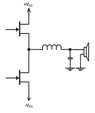
Class D Amplifier with Half Bridge
In the half-bridge type, an external LC filter is required where low-frequency signals are extracted and high-frequency signals are dissipated at the load section. Also, the benefit behind this bridge-tied load is DC blocking capacitors are not needed even with a single source of power supply. But this is not the scenario in the half-bridge type because the load fluctuates between the ground and VDD thus having a duty cycle of 50% so that the offset value equals VDD/2.

Class D Amplifier with Half-Bridge
The power range of the half-bridge device can be able to deliver efficiencies of more than 90% having the output of 14W power for each channel with 8Ω loads.
Class D Amplifier with Full Bridge
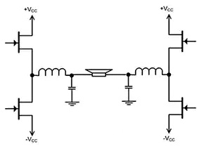
A full-bridge class D amplifier is designed using two half-bridge circuits. This configuration is also termed as bridge tied load and it functions by interchanging the conduction path across the load section so that the flow of bidirectional current happens via the load having no necessity of either a DC blocking capacitor of –ve power supply.

Class D Amplifier with Full Bridge
In full-bridge type, the offset appears at both the ends of the load section so that the flow of DC current is ‘0’. As the output signal of the full-bridge is twice that of the half-bridge, the output power enhances by 4 times.
In the construction of a full-bridge class D amplifier, twice the number of MOSFETs is required as that of a half-bridge circuit where this feature is few scenarios considered to be a drawback. But the inclusion of more switches usually corresponds that high switching losses and conduction. The power range for full-bridge devices is between 80% to 88% having an 8Ω load.
Characteristics
This section explains the class D amplifier characteristics.
- The power supply voltage range is 3.5 volts to 5 volts.
- The current consumption is 3.2 mA.
- The value of input resistance is 5.6kΩ.
- The gain is nearly 20dB.
- The standby current during Enable-Low mode is 0.82mAmps.
- The output power, when operated with a supply voltage of 5V and load with 4Ω, is a maximum of 3W.
Advantages and Disadvantages
The class D amplifier advantages are:
- Increased efficiency rate.
- Minimal heat power dissipation.
- High performance.
- Less weight.
- The battery conversion rate stays to be constant irrespective of load capacitance.
- It delivers a clear sound output and also the sound image is so precise.
- Mainly employed for mass production.
- Class D amplifiers hold unique features of remote controlling, group controlling, and monitoring.
- When compared with linear amplifiers, this switching amplifier has a high range of power efficiency.
The class D amplifier disadvantages are:
- It has no specific switch and because of this, the quality level of the entire device fails when the installed transistor and any other components do not sync up correctly.
- The output in this amplifier has a dead zone.
- The potential so close to the ground of the power transistor will swing at the time of initial connection and last shutdown procedures of the class D amplifier thus creating noise in the device.
Please refer to this link to know more about Low Noise Amplifier.
Please refer to this link to know more about DC Amplifier MCQs, Instrumentation Amplifier MCQs, Class D Amplifier MCQs
So, this is all about class D amplifier – working with applications. Here, the article focused on class D amplifier working, types, circuits, characteristics, advantages, and disadvantages. Furthermore, how electromagnetic interference shows impact while designing a class D amplifier?