As we know that communication between humans happens in multiple languages, in a similar way communication between electronic devices happens. But both the communication devices should speak the same language. The languages that the devices speak are termed communication protocols. There exist a few communication protocols such as UART communication, I2C protocol, and SPI (Serial Peripheral Interface) protocols. Today, this article let us understand the SPI protocol definition, its block diagram, Verilog code, and applications. The SPI protocol was developed in the year 1980s by Motorola and gradually appeared as the de-facto standard.
What is SPI Protocol?
SPI protocol is the communication protocol that is used for connecting low-speed devices and the devices can be RFID card readers, ADC, 2.4 GHz wireless transmitters and receivers, and memory card, readers. All these devices work with SPI protocol to establish communication with microcontrollers. This is the full-duplex synchronous serial communicating protocol where the information transmission happens concurrently from both directions.
The unique feature of this protocol is that the information transmission takes place without any intermissions. It follows a continuous stream for data transfer of ‘n’ number of bits.
Interfacing of SPI Protocol
Communication through SPI protocol takes place in a master-slave relationship. The Master acts as a regulatory device and the slave works as per the instructions received from the master. The easier configuration in SPI is a single master and single slave system whereas one master system holds the ability to control more slaves as well.
In a few scenarios, SPI is also termed as a 4-wired serial communication bus. It also has the feature of differential signaling and it offers a single simple communication way. The 4-wired serial peripheral interface protocol works with four signals which are:
- Chip selection signal/Slave selection
- MOSI – Master Out Slave In
- MISO – Master In Slave Out
- Clock
The clock signal is termed as serial clock SCK/SCLK which is generated by the master. The data transmission between slave and master is matched with this clock signal. The SPI devices have the capability of supporting a broad range of clock frequencies than that of I2C protocols. The interfacing between master and slave can be done as
- One master – One slave
- One master – Multiple slaves
The slave selection is done by the chip select signal/slave select signal where which is an active LOW signal and moves to HIGH when the slave gets disconnected from the bus. When the device works in the mode of one master and multiple slaves, then every slave should need separate chip select signals from the master.
The MISO and MOSI are the data transmission lines where MOSI has the functionality of transmitting data from master to slave and MISO has the functionality of transmitting data from slave to master. In the cases of slaves only without a master, the MOSI is termed as Serial Data In (SDI) and MISO is termed as Serial Data Out (SDO).
The below picture represents the SPI protocol architecture of single master, single master.
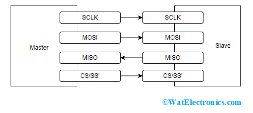
SPI Protocol Architecture
Working of Serial Peripheral Interface
As discussed that SPI device can work with one slave or multiple slaves, but has only a master. Let us look at the detailed operation and data transmission in this protocol.
CLOCK Signal
The CLK synchronizes the master output with the sampling bits of a slave. For every clock cycle, a single bit of data will be transmitted where the data transmission speed is known as the clock signal frequency. Always, the communication in SPI devices is started by the master as it generates the clock signal.
The CLK in the SPI device can be altered by clock phase (CPHA) and clock polarity (CPOL) properties. Apart from setting the clock frequency, the master should also synchronize CPHA and CPOL corresponding to the data.
Clock polarity decides the clock signal polarity. Using an inverter, the polarities can be altered. CPOL indicates that the clock signal’s base value is ‘0’ so that the idle state is ‘0’ and the active is ‘1’.
- When the clock edge is ‘0’, data transmission happens at the time of the LOW to HIGH transition. This indicates leading and trailing edges correspond to rising and falling edges.
- When the clock edge is ‘1’, data transmission happens at the time of the HIGH to LOW transition. This indicates leading and trailing edges correspond to falling and rising edges.
The clock phase decides the data timing corresponding to clock pulses. CPHA indicates that the clock signal’s base value is ‘1’ so that the idle state is ‘1’ and the active is ‘0’.
- When the clock edge is ‘0’, data transmission happens at the time of the HIGH to LOW transition.
- When the clock edge is ‘1’, data transmission happens at the time of the LOW to HIGH transition.
Slave Select (SS)
Master can select to which slave it can start communication by making slave select signal to voltage level ‘0’ on the select line. In the idle/no-transmission state, the slave select signal moves to voltage level ‘1’. When there are multiple slave select pins, then multiple slaves are in parallel connection. Whereas when a single slave select pin is present, then multiple slaves are connected to the master in daisy chain format. The below picture shows how slave select pins are connected.
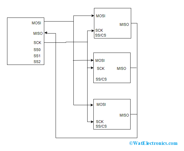
Serial Peripheral Interface With Multiple Slaves
MISO and MOSI
The master transmits data to the slave in a bit-by-bit manner using the MOSI line. The slave receives information from a master at the MOSI pin. Data transmission from master to slave is initiated with MSB bit.
The slave signal can also transmit data to the master using the MISO line. Data transmission from slave to master is initiated with the LSB bit.
Data Transmission in SPI
Initially, the master configures the clock to the frequency level (few MHz) which is supported by the slave. Then, the master chooses the slave device by making voltage level ‘0’ on the selection line. When there is a need for analog to digital conversion, then there will be a waiting period so the master has to wait before sending the clock cycles.
At every clock cycle, transmission happens in a full-duplex way where transmits one-bit using the MOSI line and slave reads that bit. In the same slave transmits one bit using the MISO line and the master reads that bit. This approach is continued even for one-directional data transmission.
Data transmissions usually require two 8-bit shift registers one for the master and the other for the slave where these registers are connected in the form of the virtual ring. Data transmission from master to slave initially happens with MSB bit. On clock edge, both the slave and master send out a bit through the transmission line. On the successive clock edge, at the receiver end, the transmitted bit gets sampled from the transmission line and sets as a new LSB of the shift register.
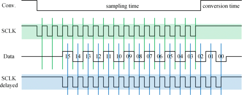
The SPI protocol timing diagram for data transmission is as follows:
When all the register bits are shifted in and out, it represents the shift register values that are exchanged between slave and master. When there is a requirement for the exchange of more information, then the reload takes place in shift registers, and the operation iterates. When the transmission completes, the master stops switching the CLK signal and deselects the slave.
This functionality is explained in the below SPI protocol block diagram.
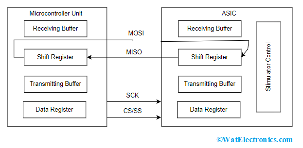
SPI Protocol Block Diagram
Serial Peripheral Interface Specifications
The specifications are:
- The clock frequency range of the SPI protocol is a maximum of 500 kHz.
- The data transmission time at a frequency of 500 kHz is 38 µ
- The digital output load at a frequency of 500 kHz is a maximum of 1 nF.
- The internal analog to digital conversion is 150 µ
SPI Protocol Arduino
To know the performance of serial peripheral interface communication between two Arduino boards, one board is configured as a master and the other board as a slave device. Master transmits logic ‘HIGH’ when the user presses the push knob. Then slave receives information from the master and as per the received information, it decides either to turn ON or turn OFF the display of the Arduino board.
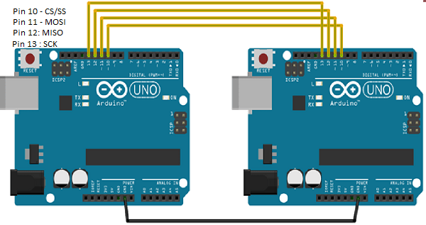
Serial Peripheral Interface With Arduino
SPI Interface as Master Arduino
#include <SPI.h>
void setup (void) {
serial.begin(115200);
disableWrite(CS, HIGH); // disables chip select pin
SPI.begin ();
SPI.setClockDivider (SPI_CLOCK_DIV8); // divides the clock by 8
}
void loop (void) {
char c;
digitalWrite (CS, LOW); // enables chip select pin
for (const char *p = “Serial peripheral Interface\r” ; c = *p; p++) {
SPI.transfer (c);
Serial.print (c);
}
digitalWrite (CS, HIGH); // disables chip select pin
delay(1500);
}
SPI Interface as Slave Arduino
#include <SPI.h>
char buffer [50];
volatile byte index;
volatile boolean process;
void setup (void) {
Serial.begin (115200);
pinMode(MISO, OUTPUT);
SPCR |= _BV(SPE);
index = 0; // buffer empty
process = false;
SPI.attachInterrupt();
}
ISR (SPI_STC_vect) {
byte c = SPDR;
if (index < sizeof buffer) {
buffer [index++] = c;
if (c == ‘\r’)
process = true;
}
}
void loop (void) {
if (process) {
process = false;
Serial.println (buffer);
index= 0;
}
}
SPI Verilog Code
module spi_state(
input wire clock;
input wire reset;
input wire [15:0] data_IN;
output wire SPI_CS_low;
output wire SPI_SCLK;
output wire SPI_DATA;
output [4:0];
)
reg [15:0] MOSI; // SPI shift register
reg [4:0] count; // control counter
reg SPI_CS_low;
reg SPI_SCLK;
reg [2:0]state;
always(@posedge clock or posedge reset)
if (reset) begin
MOSI <= 16’b0;
count <= 5’d16;
SPI_CS_LOW <= 1’b1;
SPI_SCLK <= 1’b0;
end
else begin
case (state)
0: begin
SPI_SCLK <= 1’b0;
SPI_CS_LOW <= 1’b1;
State < =1;
end
1: begin
SPI_SCLK <= 1’b0;
SPI_CS_LOW <= 1’b0;
MOSI<=data_IN[count-1];
count<=count-1;
state<=2;
end
2: begin
SPI_SCLK <= 1’b1;
If (count>0);
state<=1;
else begin
count<=16;
state<=0;
end
end
default:state<=0;
endcase
end
assign SPI_CS_LOW = CS_LOW;
assign SPI_SCLK = SPI_SCLK;
assign SPI_DATA = MOSI;
assign counter=count;
endmodule
Serial Peripheral Interface Advantages and Disadvantages
The advantages of SPI protocol include the following.
- Data streaming happens uninterruptedly.
- The slave addressing approach is simple.
- Quicker data transmission rate.
- No need for any transceivers.
- Enhanced signal integration.
- This protocol has separate MISO and MOSI lines so data transmission can be done at the same time without any waiting period.
The disadvantages of the SPI protocol include the following.
- No response whether data transmission happens or not.
- The device works only with the single master device.
- Error check possibility is absent.
- Functions only for short distances.
SPI Protocol Applications
A few of the applications of SPI protocol are as follows:
- Used in FPGA devices.
- Digital audio, and telecommunication systems.
- Employed analog to digital and digital to analog conversion systems.
Please refer to this link to know more about Modbus.
know more about Shift Register MCQs, I2C Protocol MCQs, Modbus Protocol MCQs.
This is all the concept of SPI protocol. Here the article has explained the serial peripheral interface working principle, its specifications, architecture, timing diagram, and applications. Know in detail how to connect SPI in daisy chain configuration?
