The Schottky diode, also known as a hot-carrier diode or leaky-carrier diode, is the most popular semiconductor diode invented by Walter H. Schottky in 1926. In the early days, wireless devices & metal rectifiers used cat’s whisker detectors within power applications and these detectors can be considered as primitive Schottky diodes. So, let us see why a Schottky diode is so special?
What is Schottky Diode?
A Schottky diode is a special type of metal-semiconductor junction diode that consists of a metal pad that serves as one electrode, and a metal-insulator-semiconductor(MIS) structure with a low barrier height serving as the other electrode. These diodes can have an extremely low forward voltage drop and a relatively high breakdown voltage rating. It is the first semiconductor device available that could perform the function of a rectifier with almost zero turn-on voltage.
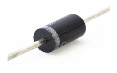
Schottky Diode
Schottky Diode Symbol
The Schottky diode symbol is shown below which is based on the basic diode symbol. But this diode symbol can be differentiated from other kinds of diode by adding two additional legs on the bar on the symbol. Similar to a normal PN junction diode Schottky diode has an anode and a cathode terminal. When a anode terminal is connected to the positive terminal and cathode is connected to the negative terminal of the voltage supply then it becomes forward bias and when anode is connected to the negative and cathode is connected to the positive terminal then it becomes reverse biased. That’s how a schottky diode is connected in a circuit.
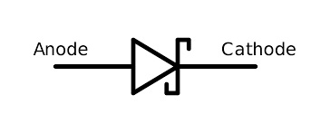
Schottky Diode Symbol
Schottky Diode Construction
A Schottky diode is constructed of a metal-semiconductor junction instead of two semiconductors as in a conventional (p-n) diode. Although it is not silicon-based like most other diodes, it still uses standard semiconductor fabrication techniques, such as alloying, diffusion, and oxidation to form its junctions. Typically, titanium or chromium is used for the metal, forming what is known as TiSb or CrSi Schottky junctions respectively.
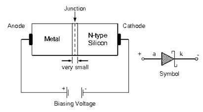
Schottky Diode Construction
The metal-semiconductor junctions are formed by depositing the metal on top of the n-doped semiconductor which creates an n-type semiconductor/metal junction. Since there are no p-n junctions, they do not display photovoltaic behaviour as in conventional. Depending on the doping the Schottky diode can be ohmic or non- ohmic.
Working of a Schottky Diode
The working principle of the Schottky diode is based on their barrier potential which is less than 0.3V. The forward voltage drop of this diode is independent of temperature and can be as small as 0.15 V (for an idealised semiconductor/metal interface), compared to 0.6 – 0.7 V for silicon p–n diodes and 0.3 V for germanium p–n diodes. The turn-on voltage of the device is generally not constant; it decreases with increasing current through the device and also depends on the reverse voltage applied to the device.
This effect is sometimes undesirable since it means that the forward resistance of this diode does not remain constant when it is used at high frequencies, or when it passes high currents in circuits where there are other sources of forwarding voltage drop (such as the resistances of wires and printed circuit tracks.
Since these diodes have no PN junction, they do not exhibit the reverse recovery time associated with other diodes when switching from conduction to non-conduction states. This allows them to switch much more quickly, allowing higher frequencies to be used. They also have no stored charge in the depletion region so suffer less from thermal runaway than PN junctions do under high current conditions.
Schottky Diode Circuit
Generally, this diode works like a normal diode but the unique characteristics of this diode are high switching speed & very low voltage drop. To understand this in a better way, let us connect a Schottky diode in a circuit and check how it functions.
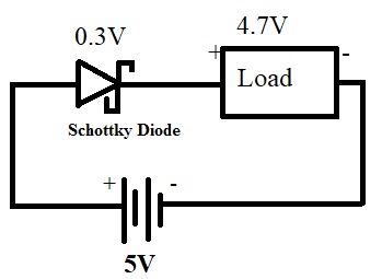
Schottky Diode Circuit
In the above circuit diagram, the Schottky diode is connected with the load. This circuit is mainly used for differentiating the voltage drops. So Schottky diode circuit is powered with 5 Volts. Once current supplies through this diode then it will have only 0.3V voltage drop & leave the remaining 4.7 volts for the connected load. So the voltage drop of this diode is less has a lower voltage drop. This diode also has some benefits like less noise, better performance, faster switching rate as compared to the PN-junction diode.
Schottky Diode VI Characteristics
The current-voltage characteristic of a Schottky diode is nonlinear with a negative temperature coefficient. This diodes VI curve simply looks like a PN junction diode but is much steeper. The VI characteristic diagram of the Schottky diode is shown below.
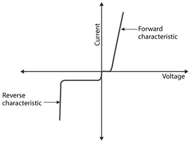
VI Characteristics
- The forward voltage drop of this diode is extremely low as compared to the PN junction diode.
- The forward voltage drop of this diode ranges from 0.2 to 0.3 volts and it is normally designed with silicon.
- The reverse saturation current mainly occurs at a very less voltage as compared to Si diode.
How to connect a Schottky diode
In this section, we will see how to connect this diode in different applications like an RF detector, clamper and switching circuit, etc. Please refer to this link for Choosing resistor values for diodes.
Schottky Diode as an RF Detector
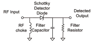
The figure below shows the circuit diagram of a Schottky diode used as an RF detector. The circuit is designed for detecting signals in the range of 500 kHz to 1 MHz. The RF signal will be applied at the input through capacitor C1 and resistor R1.
Detector Circuit
Here, When the RF input signal (AC signal ) is the applied to the diode , the Schottky diode gets forward bias during the positive half cycle. This charges the capacitor. During the negative half cycle the diode get reverse biased so the output of the signal will be a D.C. signal with the same voltage as the input. But When the input voltage decrease the capacitor discharges through the filter resistance.
These circuits are simple rectifier circuits that produce a low-frequency o/p voltage or current which is proportional to the input RF signal. These circuits are frequently used to check the output range of a power amplifier within a radio transmitter, otherwise, they can just specify the existence or deficiency of an RF signal.
Schottky Diode as a Switch
To use a Schottky diode as a switch, you need to know the forward voltage drop V_F that the diode exhibits. This is usually specified in the datasheet and depends on temperature, current, and height of voltage drop.
For example, if you want to use a Schottky diode as a switch in a circuit to turn on an LED when the input signal is 5 volts or greater, you need to know the forward voltage drop V_F of your LED. Let’s say it’s 2.8V_F. If you connect the LED directly with 5V it will blow up. You need 3.2V at least to turn it on (5V – 2.8V = 3.2V).
Schottky Diode as a Clamper Circuit
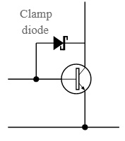
The Schottky diode can be used as a clamp diode within a transistor circuit to enhance the operation once used as a switch. The Schottky diode is connected in between the base and collector terminals of the transistor to function as a clamp. To generate a low logic output as ‘0’, the transistor is turned ON, so the BE junction of this transistor is forward biased.
Clamp Diode Circuit
Once the diode uses most of the current & permits the transistor’s turn-off time to be greatly reduced, thus the circuit speed can be enhanced. The Schottky diode is simply used in several applications like in both high power rectification & very low power signal detection.
Schotty Diode in the Logic Circuit
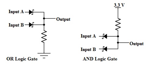
The traditional way to make a logic gate is to use transistors and logic gates. But these logic gates have many disadvantages, such as the fact that they are slow and they take up a lot of space on the motherboard. Whereas when made with a Schottky diode it has very small and provides a faster out. It can be used in place of an inverter. This means that a Schottky diode can be used to make an AND gate or an OR gate.
OR Gate & AND Gate
As shown in the above AND logic gate, a 2-input AND gate can be formed by using two Schottky diodes like A & B. The working of AND gate follow as; If both the inputs are logic zero then the output will be logic and if the two inputs are logic 1 then the output will be 1. To form an AND gate the Schottky diode is connected in reverse bias so when a 5v is applied to both gates it is reverse biased and does not conduct and so the output if be high. If any one of the input is low then that diode conducts and so the output is low.
In the above OR logic gate circuit, two Schottky diodes can be used to form a 2-input OR logic gate. The OR gate working is; if any one of the inputs like A & B is high then only the output will be high. If both the inputs are low then the output will be low. In case of OR Gate the schottky diode is connected in forward bias condition so if any one of the input is high the diode conducts and so the output is high.
Difference between the Schottky Diode and a Normal Diode
The difference between the Schottky diode & a PN junction diode includes the following.
| Schottky Diode | PN Junction Diode |
| The semiconductor diode can be formed through the semiconductor junction with a metal. | A PN-junction diode can be formed once a p-type semiconductor is merged to an n-type semiconductor for creating a potential barrier voltage across the junction of the diode. |
| The forward current in this diode mainly occurs because of the thermionic emission or transport of the majority charge carrier. | The forward current in the PN junction diode mainly occurs because of the diffusion currents or transport of minority change carriers. |
| The reverse current in this diode can be produced simply because of the majority carriers to overcome the barrier. | Its reverse current within the PN junction diode can be produced because of the minority charge carriers’ diffusion into the depletion layer & drifting to the other face. |
| The current in voltage of this diode is very small like 0.3V | The current in voltage of this diode is large 0.7V |
| The switching speed of this diode is high. | The switching speed of this is low. |
| The ideality factor of this diode is 1. | The ideality factor of this diode ranges from 1.2 to 2. |
| These diodes are available in two types rectifying & non-rectifying type. | PN junction diodes are available in different types like LED, Photodiode, Zener diode, etc. |
| The low reverse voltage of this diode ranges from 10 to 1400V. | The low reverse voltage of the PN junction diode ranges from 20 to 60V. |
| The forward voltage drop of this diode is lower like 0.3V. | The forward voltage drop of the PN junction diode is 0.6 TO 0.7 V. |
Advantages
There are two major advantages of a Schottky diode over an ordinary p–n junction diode
- The forward voltage drop is lower, typically 0.15 to 0.45 volts (compared to 0.6 to 1.5 volts for a standard silicon diode) so it can operate at higher frequencies than the PN Junction diodes.
- The switching action is faster due to the lack of a built-in potential (depletion layer) that exists in p–n junction diodes which prevents electrons and holes from diffusing across the space between the N and P semiconductor regions., and their capacitance is considerably lower making them suitable for high-speed switching applications.
Disadvantages
The disadvantages of the Schottky diode include the following.
- The reverse recovery time is also relatively slow.
- They are more expensive than conventional PN junction silicon diodes.
- It is also susceptible to thermal degradation at high temperatures.
- It is also harder to make compared to other diodes.
- These diodes are less stable than conventional diodes in extreme temperature and high-radiation environments, due to the fact that the metal-semiconductor junction has an asymmetric current-voltage characteristic, unlike the symmetric characteristic of a p-n junction.
Please refer to this link for Schottky Diode MCQs
Applications
The applications of the Schottky diode include the following.
- There are quite many applications of this diode like power supply rectification, wave-shaping, frequency conversion, etc.
- The main use is in power supply applications such as switched-mode power supplies because they have lower forward voltage drop than normal diodes. This reduces conduction losses and makes them more efficient.
- They are commonly used as RF mixers and detectors in radio receivers, as ring mixer multipliers in microwave transmitters, and for various other applications such as clamping, voltage clamping, and free-wheeling diodes.
- They have used clock buffers in digital integrated circuits to reduce power consumption by reducing the current drawn from the power supply during the low state of a clock signal.
Thus, this is all about the importance of Schottky Diode. These diodes are available with different package types, including SMD (surface mount), radial led, and axial led. There are different parameters that need to consider while selecting Schottky diode like forwarding voltage drop, reverse breakdown voltage, reverse recover time & reverse leakage current. Here is a question for you, what is Zener Diode?