We all know that logic gate is the idealized computational approach for the implementation of a Boolean function which is either performed on a single or more number of inputs thus generating single output. As per this context, the term can be referred to as an ideal logic gate or non-ideal physical device. These logic gates are basically designed using transistors, relay logics, diodes, and many other mechanical elements. The very fundamental type of logic gates is AND, OR, and NOT gates. Along with these, we have NAND gate and NOR gates which are termed Universal Logic Gates.
Charles Peirce demonstrated that either NOR or NAND logic gates are enough to reproduce the operation of other logic gates, but his demonstration was left unpublished till 1933. Then, the initial proof of publication happened in 1913 by Henry M. Sheffer and the functionality of NAND is termed as Sheffer stroke. And today, this article focuses on explaining NAND gate definition, circuit, truth table, its applications, and advantages.
What is NAND Gate?
NAND gate also called Negated AND, NOT AND is the combination of AND and NOT gates which are in series connection. The NAND gate is one of the universal logic gates because with the universal gates any other fundamental operations can be accomplished. Therefore, the combination of NAND and NOR gates can give AND, OR, and NOT gates.
This gate gives the output HIGH when both the inputs are at logic LOW or when either of the inputs is at a logic LOW state. It can also be defined as that the output is LOW only when both the inputs are HIGH.
The NAND gate Boolean expression is given by:
A = (X. Y)’
Here, X and Y are the inputs and A is the output. NAND logic gate can be achieved by multiplying all the inputs and then complementing the multiplied result.
The NAND gate symbol is shown as follows:
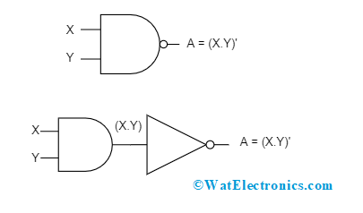
Basic NOT AND Gate
NAND Gate Types
There are basically three types of NAND logic gates depending on the number of inputs. Those are explained below:
2-input NAND
Here, the gate accepts two inputs and gives single output which is the basic formation of NAND gate. Here, the total possible combinations of inputs are 4. The 2-input NAND gate truth table is shown below:
| X | Y | A |
| 0 | 0 | 1 |
| 0 | 1 | 1 |
| 1 | 0 | 1 |
| 1 | 1 | 0 |
3- input NAND
Here, the gate accepts three inputs and gives single output. Here, the total possible combinations of inputs are 8. This three-input logic gate can be formed by combining any number of individual inputs The 3-input NAND logic gate truth table and logical design is shown below:
| A | B | C | X |
| 0 | 0 | 0 | 1 |
| 0 | 0 | 1 | 1 |
| 0 | 1 | 0 | 1 |
| 0 | 1 | 1 | 1 |
| 1 | 0 | 0 | 1 |
| 1 | 0 | 1 | 1 |
| 1 | 1 | 0 | 1 |
| 1 | 1 | 1 | 0 |
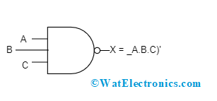
3 Input NAND
Multi-Input NAND
Similar to multi-input OR and AND gates, an n-input NAND logic gate can also be formed. When the number of inputs is odd, the unused input signal is kept high by connecting this unused signal to the power supply through pull-up resistors.
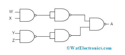
Multi Input NOT AND
Below is the logical expression and NAND gate design for 4-input NAND.
| W | X | Y | Z | A |
| 0 | 0 | 0 | 0 | 1 |
| 0 | 0 | 0 | 1 | 1 |
| 0 | 0 | 1 | 0 | 1 |
| 0 | 0 | 1 | 1 | 1 |
| 0 | 1 | 0 | 0 | 1 |
| 0 | 1 | 0 | 1 | 1 |
| 0 | 1 | 1 | 0 | 1 |
| 0 | 1 | 1 | 1 | 1 |
| 1 | 0 | 0 | 0 | 1 |
| 1 | 0 | 0 | 1 | 1 |
| 1 | 0 | 1 | 0 | 1 |
| 1 | 0 | 1 | 1 | 1 |
| 1 | 1 | 0 | 0 | 1 |
| 1 | 1 | 0 | 1 | 1 |
| 1 | 1 | 1 | 0 | 1 |
| 1 | 1 | 1 | 1 | 0 |
Transistor Implementation of NAND
To design a NAND gate using transistor, mostly two bipolar junction transistors are needed. Here, this logic gate is constructed using two NPN transistors, 10k Ohms resistors – 2, 2-4k Ohm resistor 1, push buttons – 2, wires to establish connections between the components, LED display, and power supply. Below is the NAND gate circuit diagram that explains the functionality.
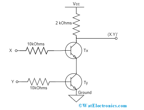
NAND Gate Using Transistor
As per the above diagram, the two NPN transistors Tx and Ty are in series connection and the circuit connection is the same as AND gate. The collector end of Tx has a connection with the power supply using a 2k Ohm resistor and it is also connected to the output. Whereas the emitter end of Tx is connected to the collector end of Ty so that both the transistors are in series connection.
Then the emitter end of Ty is connected to the ground and this completes the circuit connection. On the other hand, the base ends of both Tx and Ty are connected to inputs X and Y through 10k ohm resistors correspondingly.
To know the exact functionality of the Negated And logic gate using a transistor, we need to analyze all four combinations of inputs.
Please refer to this link to know more about NAND Gate MCQs
Case 1: When X = 0 and Y = 0
When both the inputs are LOW, then the two transistors Tx and Ty operating as the switch do not permit for connection between emitter and collector ends. Because of this, when there is a power supply across the circuit, the current will not pass to the emitter end of Tx and it passes only to the collector end of Tx. As the collector end is even connected with LED, this power supply directly reaches to LED and the LED glows making the output as HIGH.
Case 2 : When X = 0 and Y = 1
When the Y input is at logic HIGH, the base end of Ty establishes a connection between its emitter and collector ends. Whereas, the input at the collector end for Ty is 0 which means there exists no connection in between the emitter and collector ends of Tx. Because of this, the power supply that passes to the collector end reaches to output making the LED display ON i.e. output is HIGH.
Case 3: When X = 1 and Y = 0
When the X input is at logic HIGH and Y input is at logic LOW, the switch for Tx moves to ON and Ty becomes OFF. This makes the output as logic HIGH which is similar to case 2.
Case 4 : When X = 1 and Y = 1
Here, the inputs X and Y are at logic HIGH this means the power supply directly reaches to collector end through 2k Ohm resistor. As both the inputs are at a HIGH state, this establishes a direct connection between the collector end of Tx and the emitter end of Ty. Whereas Ty is connected to the ground, the potential variation in between the collector end of Tx and emitter end of Ty becomes ‘0’. As the collector also has a connection with output, the LED display gets 0V i.e. the output is LOW.
Deriving Basic Gates Using NAND Logic Gate
As it is already discussed that NOT AND gate is a universal gate. This makes it more flexible that any basic logic gate can be derived using a NAND gate. The below section explains on NAND gate to derive basic gates.
AND using NAND
When the inputs are considered as X and Y, then for an AND gate, the desired output is X.Y. So, this Boolean expression is derived using the Negated And logic gate.
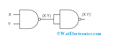
AND Using NOT AND Gate
Using the Involution principle,
- Y = ((X.Y)’)’ = X. Y
OR using NAND
When the inputs are considered as X and Y, then for an OR gate, the desired output is X + Y.
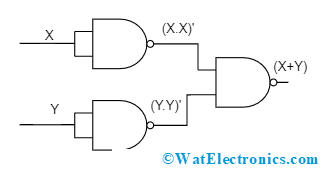
OR Using NOT AND Gate
So, this Boolean expression is derived using NAND logic gate.
Using Involution principle,
X + Y = (X +Y)’
- [(X + Y)]’
- [(X.X)’(Y.Y)’]’ -> Idempotency principle
NOT using NAND
When the input is considered as X, then for a NOT gate, the desired output is X’. So, this Boolean expression is derived using the NAND logic gate.

NOT Using NOT AND Gate
Using the Idempotency principle,
(X.X)’ = (X)’
NAND Gate IC
The commonly existing ICs of NAND gate are:
In TTL logic we have,
- 74LS00 Quad 2 – input NAND IC
- 74LS10 triple 3 – input NAND IC
- 74LS20 Dual 4 – input NAND IC
- 74LS30 single 8 – input NAND IC
In CMOS logic we have,
- CD4011 Quad 2 – input NAND IC
- CD4023 Triple 3 – input NAND IC
- CD4012 dual 4 – input NAND IC
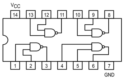
74LS00 IC
This is a two-input NAND gate IC that has 14 pins. The IC consists of 4 independent gates where each gate performs Negated AND logic gate functionality. These gates work on advanced silicon gate CMOS technology to gain higher functional speeds utilizing minimal power and every gate has buffered outputs. The 74LS logic family is in compatibility with the 74HC family in regards to functionality and pin-out. The inputs of every gate in the IC are safeguarded from damage because of static discharge by internally present diode clamps to the power supply and ground.
The functional characteristics of 74LS00 are:
Operating voltage ranges between 4.75 V to 5.25 V
- The LOW and HIGH levels of input voltages are 0.8 V and 2 V
- The HIGH and LOW levels of output currents are -0.4 mAmps and 8 mAmps
The electrical characteristics are:
- The HIGH and LOW-level input currents are 20 µAmps and -0.36 µAmps
- The HIGH and LOW-level output voltages are 2.7 V and 0.5 V
The switching characteristics of 74LS00 are:
- The output propagation delay time at the level of LOW to HIGH has a minimum of 3 ns and a maximum of 10 ns at a CL of 15 pF and minimum of 4 ns and a maximum of 15 ns at a CL of 50 pF
- The output propagation delay time at the level of HIGH to LOW has a minimum of 3 ns and a maximum of 10 ns at a CL of 15 pF and minimum of 4 ns and a maximum of 15 ns at a CL of 50 pF
VHDL Code of NAND Logic Gate
This section explains the VHDL code implementation for a NOT AND logic gate:
library IEEE;
use IEEE.STD_LOGIC_1164.ALL;
use IEE.STD_LOGIC_ARITH.ALL;
use IEEE.STD_LOGIC_UNSIGNED.ALL;
entity NAND Gate is
Port ( X : in std_logic;
Y : in std_logic;
A : out std_logic);
end NAND Gate;
architecture NAND1 of NAND Gate is
begin
A <= X NAND Y;
end NAND1;
NAND Gate Applications
There are various applications of NAND gate in real life where few of those are explained below:
- Used in alarm circuits through light detection radiation
- Employed in freezer warning buzzer devices
- NAND logic gates are utilized in automatic temperature regulation circuits
- These are used for analyzing the status of the sensor that is connected to various doors and windows.
- Used in burglar alarms.
Advantages and Disadvantages
The NAND gate advantages, disadvantages are as follows:
Advantages
- NAND gates are cost-effective devices and they have more storage capacities as per their size.
- This gate offers good replaceability which means that when the flash memory gets damaged, then it can be replaced with a suitable component.
- The memory ability of NAND can substitute huge files like USB drives, digital cameras, and tablets.
- High endurance and durability.
Disadvantages
- When compared with the NOR gate, the NAND memory architecture and speed are less reliable.
Please refer to this link to know more about OR Gate Advancements.
This is all about an overview of the NAND logic gate. This article has given detailed exposure to the NAND gate truth table, circuit, design, applications, and advantages. Also, know how CMOS logic NAND are constructed and what are their performance characteristics?
