In any of the digital circuits, the primary device that holds more prominence is the logic gate. The name logic gates come from the capability of those devices to provide outputs depending on multiple combinations of inputs. These logic gates are mainly categorized as basic logic gates, special purpose, and universal gates. The one basic gate which we are going to discuss today is NOT gate. The inventor of NOT gate was George Boole and he also invented the concept of boolean logic. Today, this article helps us in knowing the functionality of the inverter, its circuit, design, applications, benefits, and limitations.
What is NOT Gate?
NOT gate is also called an inverter gate where it inverts the input signal that is applied to it. This is the single input and single output gate. Here, inversion corresponds that logic ‘0’ to be converted into logic ‘1’ and logic ‘1’ converted to logic ‘0’.
The NOT gate symbol is in the form that it has a triangle having a bubble at the end. This bubble is termed an inversion bubble which provides the complemented signal of input. This gate is also called a decision-making gate due to the reason that it has only single input.
In this inverter logic gate, the bubble can also be present on the input side of the gate which represents an active less input signal. This inversion of the input in the inverter is not just bound to the gate, it can even be implemented for any other gates or in many digital circuits, and either it can be at input or output signal.
For example, when the input signal is considered as X, then the output of the inverter gate is X’. Similarly when the value of the input signal is ‘1’, then the output is ‘0’ and vice versa. The NOT gate symbol is shown below:
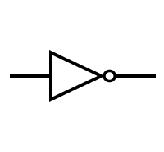
Symbol of NOT gate
As truth table lists out the outputs for all the combinations of applied input signals. Below is the NOT gate truth table
| Input | Output |
| X = 0 | X’ = 1 |
| X = 1 | X’ = 0 |
The functionality can be clearly explained with the below NOT gate circuit diagram.
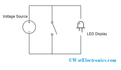
Symbol of inverter gate
The picture shows that the LED device will glow when switch S is in an OPEN state and it moves to OFF when switch S is in the CLOSED state.
NOT Gate using Transistor
The NOT logic gate can be easily implemented through the bipolar transistor. Below is the diagram that shows inverter implementation using a transistor.
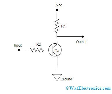
NOT Gate Using Transistor
Case 1:
When high voltage is applied as input to the inverter which is Vcc = +5V. Here, the transistor Tx receives the required amount of potential to move into ON condition. When the transistor moves into the ON state, the voltage at B terminal will have a path to the earth via resistor R1.
Now, the transistor will be in short-circuited condition, so that all the Vcc voltage gets dropped at R1 and no voltage appears at the output terminal which is ideally ‘0’ volts.
In general, there happens some amount of voltage drop at the emitter and collector terminals which is approximately 0.6V. So, the entire supply voltage will not be dropped at the resistor it is 5-0.6 = 4.4 Volts. So that 0.6V is almost considered as ‘0’ or logic ‘0’.
Case 2:
When a low voltage (0V) is applied as input to the inverter then the transistor’s base terminal is provided with 0V or it is grounded.
Now, the transistor Tx moves into OFF condition and the supply voltage has no path to move to earth and the entire voltage will be at the output terminal which means that the output is at logic HIGH.
Not Using NAND Gate
To derive inverter circuit from NAND, it has to be considered that both the inputs of the NAND gate are connected which is taken as a single input to the NAND gate. With this connection, when the input was passed through two-input NAND gates, then it results in a complement of the input signal. This represents a logical negation of the input which is the operation of NOT gate. Below is the logical diagram that shows an implementation of an inverter circuit using NAND gate.

NOT Using NAND
As per the Idempotency principle,
(X. X)’ = (X)’
So, (X.X)’ = X’
NOT Logic Gate using NOR Gate
To derive NOT gate using NOR, it has to be considered that both the inputs of NOR gate are connected which is taken as a single input to NOR gate because NOT has a single input. Here, the IC 7402 is used which is a quad 2-input NOR gate. So, when a binary HIGH input is given as input, the result is logic LOW and in the same way, when a binary LOW signal is provided as input, the output is logic HIGH.
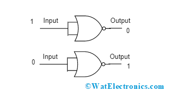
NOT Using NOR
Inverter using Multiplexer
To implement NOT gate using mux, the only thing to do is the enable the inverting path. This happens when the A0 pin in the mux is connected to 1 and the A1 pin is connected to 0. It can also be said that the signal ‘0’ has to be propagated to output when the input signal is ‘1’ and signal ‘1’ has to be propagated to output when the input signal is ‘0’. The below diagram shows the implementation of NOT gate using mux.
| S | Y |
| 0 | 1 |
| 1 | 0 |
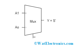
NOT Using Multiplexer
Y = S’A0 + SA1
= S’ . 1 + S. 0
Y = S’
NOT Gate Inverter IC
The IC number for the inverter device is 7404 which is a high-speed CMOS technology quad input one. This IC consists of 6 individual NOT gates which all are considered as single packages. This IC is termed a hex inverter because it contains 6 separate inverters and the outputs are directly interfaced to TTL, NMOS, and CMOS.
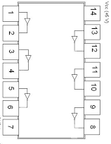
IC 7404
The voltage levels required for NOT gate IC are:
The supply voltage Vcc ranges between 4.75 to 5.25 volts and the nominal voltage range is 5V.
The minimum level of HIGH input voltage VIH is 2V
The maximum level of LOW input voltage VIL is 0.8V
The maximum level of HIGH output current IOH is -0.4 mAmps
The minimum level of LOW output current IOL is 16 mAmps
The pin description of 7404 NOT gate IC is
Input terminals
1 – Input of gate 1
3– Input of gate 2
5 – Input of gate 3
9 – Input of gate 4
11 – Input of gate 5
1 3– Input of gate 6
Output terminals
2 – output of gate 1
4 – output of gate 2
6 – output of gate 3
8 – output of gate 4
10 – output of gate 5
12 – output of gate 6
Common terminals
7 – ground pin which is connected to ground
14 – Vcc pin which supplies positive voltage to the IC
VHDL Code of Inverter
This section explains the implementation of NOT gate in a VHDL code
Step 1: Initially, the libraries are imported
Step 2: Then the entity is stated as NOT gate and also input and outputs are declared as X and Y
Step 3: After the declaration of the entity, the architecture of the declared entity has to be defined. Here, the architecture of NOT gate entity is given as “architecture not Logic of NOT”. As we know Y is considered as output which is nothing but NOT functionality for input X. So, Y is mapped with X which is Y <= NOT(X). Then the architecture is closed by “end notLogic”.
The VHDL code implementation of NOT gate is:
library IEEE;
use IEEE.std_logic_1164.all;
entity NOT is
port (X : in std_logic;
Y : out std_logic );
end NOT;
architecture notLogic of NOT is
begin
Y <= not (X);
end notLogic;
Electronic Execution of Inverter Logic Gate
The inverter circuits can even be implemented through NMOS, and PMOS transistors coupled with resistor components. As the resistive drain techniques use only one transistor, the NOT gate design can also be done at minimal prices. Though the flow of current in the resistor happens in two states, this resistive drain technique is not implemented for high processing speeds and utilizes more power.
As an alternative, inverters are designed with the help of complementary configurations in the CMOS technology. With this configuration, power usage can be reduced because one transistor will be always in the OFF state in both the logic states.
The processing speed can be enhanced because of comparatively less resistance when compared with the only NMOS or only PMOS approaches.
These gates can also be designed using BJT devices either in TTL or RTL configurations. The below picture shows the implementation of the inverter in NMOS, PMOS, static CMOS, NPN RTL, and NPN TTL configurations.
The analytical illustration of inverter can be given as:
f(x) = 1 – x
where
f(0) = 1 – 0 = 1
f(1) = 1 – 1 = 0
Hex Inverter
Based on the above discussion, we came to know that an inverter circuit can also be designed through a transistor. Whereas transistors require some amount of time for switching between ON and OFF states. The switching phenomenon takes place with some hold-up time in the transistors and this does not happen instantly. Also, the transistor holds the foremost feature of amplification that directs to its functionality in this mode.
In the linear amplification functionality, a minimal variation in the input corresponds to the corresponding variation in the output and this also leads to switching between ON and OFF states suddenly. In order to get rid of these complications, a Hex or Schmitt inverter is designed.
As we know, in the TTL configuration, 2 – 5 volts is taken as HIGH logic and 0 – 0.8 volts is taken as LOW logic. Here, 2 volts and 0.8 volts are set to be Upper and Lower Threshold Voltage levels (UTV and LTV). The functionality of the Schmitt inverter takes place based on the limits of UTV and LTV and varies its state abruptly. When there is a rise in the input voltage more than the UTV level, then the output of the Schmitt inverter alters to LOW logic and in the same way when there is a drop in the input voltage below the LTV level, then the output of the Schmitt inverter alters to HIGH logic.
This holds the preceding state at the time of the transition period and varies its state quickly when the threshold voltage is reached. This is termed Hysteresis which is inbuilt in the Schmitt inverter.
The pictorial representation of UTV and LTV limits along with the output waveform is shown below:
Performance Analysis
The performance of the inverter circuit is calculated through a voltage transfer curve where the curve is plotted against input and output voltages. With this VTC curve, the parameters like functional logic levels, gain, noise levels can also be measured.
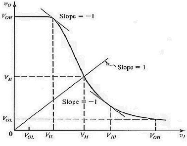
VTC Curve of Inverter
Mostly, the VTC curve appears as an inverted step function where this represents the exact switching of OFF and ON states, whereas in the real scenario a steady transition location also exists. The VTC curve represents that for minimal voltage levels, the output is high and vice versa.
The transition in the slope is considered a quality measurement. And when it is steep, it results in exact switching measurement. The noise tolerance can even be calculated by relating the minimum and maximum levels of input and output for every functional region of ON and OFF.
Applications
The foremost NOT gate application is in the CMOS inverter for the generation of waveforms.
- Employed in temperature detection devices.
- Used in daily usage devices like desktops, tablets, and mobiles.
- Complex devices such as decoders, state machines, and multiplexers also use inverter circuits.
- Used in a crystal oscillator.
NOT Gate Advantages and Disadvantages
The benefits are:
- Inverter devices can be constructed at a low cost.
- Requires minimal power consumption for its operation.
- Enhanced processing speed.
Can be constructed in RTL and TTL configurations
The drawbacks are:
- It has an only single output and is not suitable for the requirement of providing two inputs
- There is the limited operational voltage level
Please refer to this link to know more about Open Drain.
And, this is the detailed information of NOT gate. This article has provided a clear overview on defining inverter, truth table, circuit, implementation using mux, benefits, and drawbacks. Know, how an inverter is used in a crystal oscillator device?

