When a p-type and n-type interfaced together that leads to the formation of a PN Junction. The commonly suggested semiconductor for this p-n junction is either silicon or germanium based on its preferred electrical properties and its abundance. Basically the p-type and n-type of a semiconductor is formed due to doping impurities.
There is an interesting concept evolved from it clearly states that both the p and n regions are conducting until the formation of a barrier. Once it has been formed the p and n regions become neutral in terms of conduction. This evolving concept has been utilized for the development of modern electronics.
The Theory Behind The Formation of PN Junction
Based on the required conditions one can easily say that there are two types of materials involved in a single crystal to interface in such a way that PN Junction has formed. P-type is formed because of trivalent doping impurity.
These impurities accept free electrons and they become negatively charged ions. Similarly n-type is formed by doping it with pentavalent impurity and donates the free electrons in order to become positively charged ions.

general-representation-of-p-n-junction
Rather than using the same material if we use different semiconductors for the formation of the PN Junction there will be a phenomenon of scattering that inhibits the flow of charge carriers. Because of this reason single crystal with doping concept is preferred.
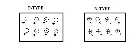
Charge Representation of P-Type and N-Type
As the p and n-type semiconductor have been interfaced or fused together in such a way that at the center there must be action between majorities of the charge carriers that tend to the formation of the junction in between them.
Now, there are charges in both p and n-types. P-type consists of holes as majority charge carriers and n-type have electrons as the majority. When these types are in contact with each other there majority carriers tend to move and the process of diffusion occurs. This is only possible when n-type and p-type both are formed on a single crystal.

charge-representation-of-p-type-and-n-type
As the charges flow from higher concentration to lower concentration and the process impacts in such a way that some charge has been imposed at the center on the impure ions. These carriers form a layer that is static and adjacent towards the junction. Then this static layer becomes so strong in terms of electric charge that towards n-type electrons lied statically while p-type has holes for that purpose.
However, the concentration will be on the major part but there will be some minority carriers in each region showing the impact of their presence. As p-type has minority carriers as electrons it tends to move and crosses the PN Junction and gets combined in n-type region. A similar concept is also applied for n-type minority carriers. As a result, the regions tend to attain the condition of neutrality.
This makes the junction to attain a state of equilibrium. In this state, the donor tends to oppose holes and the acceptors repel the electrons. This phenomenon leads to the formation of a zone called “potential barrier”. The barrier doesn’t have any free carriers left it means that all the free electrons are combined by respective holes in it.
Please refer to this link to know more about PN Junction Diode MCQs
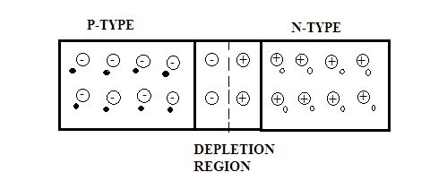
Interaction of N-Type and P-Type
As a result, there must not be any free carriers across both p and n-types junction. Then both p and n regions are now termed as neutral regions. In other words, these free carriers are depleted. Hence the region of the p-n junction is termed as Depletion region and the charge will be neutral on both sides.

interaction-of-n-type-and-p-type
In the formation of depletion layer n-type loosen its free electrons while p-type has lost free holes. Both the sides have some ions and its nature is impure. This results in the existence of an electric field in it. The problem is, in order to overcome the barrier it requires some extra charge. Hence the electric field generated due to the process of diffusion without any application of power supply is can be given as
Here ND represents the donor impurity concentration; NA represents the acceptor’s impurity concentration. Where ni refers to the intrinsic concentration.
Once the barrier is formed at the center there is the existence of the other two processes. Firstly, the concentration of the carriers is different and when the holes tend to diffuse from p-type to n-type there some current has been generated at the junction termed as diffusion current. Secondly, because of this depletion, there is some movement in minority carriers in such a way that electric field is imposed because of this electron from p-side tends to flow towards n-side resulting in drift current.
Diffusion current is possible only by the movement of majority carriers whereas drift is possible by the influence of minority carriers. After the formation of a barrier if charges require movement then it is possible by applying it with suitable voltages. This concept is termed as biasing. Without any power supply, there is the presence of some potential in the semiconductor based on its relevance.
If it is silicon then it has 0.6-0.7 volts as the basic potential across the depletion region. In case germanium is used then it has 0.3-0.35 volts. As it is referred to potential barrier it opposes the flow of charge carriers on both sides of the junction. The PN Junction barrier is formed during the process of manufacturing itself compared to germanium silicon has the highest barrier potential. This potential is highly sensitive to the variations in the temperature, the element or material utilized in its fabrication as well as the concentration of doping required based on the type and the factors.
The most major factor of inbuilt potential inside the interfaced PN Junction is responsible for repelling the flow of electrons and holes once the barrier has formed. The flow of charged particle in such interfacing will always be in a unified direction. This is a huge application
These PN Junction devices are considered as the fundamental units for any type of transistors, a few modifications in it can be used for various purposes based on requirements. Now, these are the basics that made p-n junction more popular in all the aspects termed for modern electronics. Have you ever thought of how and when these types of p or n-types are replaced and utilized in any other respective equipment?