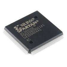
FPGA
Electronic industry has simulations and prototyping as their important segments since a long period. Electronic companies design the hardware dedicated to their products with their standards and protocols which makes it challenging for the end users to reconfigure the hardware as per their needs. This requirement for hardware led to the growth of a new segment of customer-configurable field programmable integrated circuits called FPGAs. In this article, we discuss FPGA Architecture and Applications.
What is FPGA?
The FPGA is Field Programmable Gate Array. It is a type of device that is widely used in electronic circuits. FPGAs are semiconductor devices which contain programmable logic blocks and interconnection circuits. It can be programmed or reprogrammed to the required functionality after manufacturing.
Basics of FPGA
When a circuit board is manufactured and if it contains an FPGA as a part of it. This is programmed during the manufacturing process and further can be reprogrammed later to create an update or make necessary changes.
This feature of FPGA makes it unique from ASIC. Application Specific Integrated Circuits (ASIC) are custom manufactured for specific design task. In past FPGAs are used to develop low speed, complex and volume design, but today FPGA easily pushes the performance barrier up to 500MHz.
In microcontrollers, the chip is designed for a customer and they have to write the software and compile it to hex file to load onto the microcontroller. This software can be easily replaced as it is stored in flash memory.
In FPGAs, there is no processor to run the software and we are the one designing the circuit. We can configure an FPGA as simple as an AND gate or a complex as the multi-core processor.
To create a design we write Hardware Description Language (HDL), which is of two types – Verilog and VHDL. Then the HDL is synthesized into a bit file using a BITGEN to configure the FPGA.
The FPGA stores the configuration in RAM, that is the configuration is lost when there is no power connectivity. Hence, they must be configured every time power is supplied.
FPGA Architecture
FPGAs are prefabricated silicon chips that can be programmed electrically to implement digital designs. The first static memory based FPGA called SRAM is used for configuring both logic and interconnection using a stream of configuration bits. Today’s modern EPGA contains approximately 3,30,000 logic blocks and around 1,100 inputs and outputs.
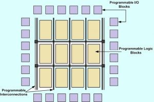
FPGA Architecture
The FPGA Architecture consists of three major components
- Programmable Logic Blocks, which implement logic functions
- Programmable Routing (interconnects), which implements functions
- I/O blocks, which are used to make off-chip connections
Programmable Logic Blocks
The programmable logic block provides basic computation and storage elements used in digital systems. A basic logic element consists of programmable combinational logic, a flip-flop, and some fast carry logic to reduce area and delay cost.
Modern FPGAs contain a heterogeneous mixture of different blocks like dedicated memory blocks, multiplexers. Configuration memory is used throughout the logic blocks to control the specific function of each element.
Programmable Routing
The programmable routing establishes a connection between logic blocks and Input/Output blocks to complete a user-defined design unit.
It consists of multiplexers pass transistors and tri-state buffers. Pass transistors and multiplexers are used in a logic cluster to connect the logic elements.
Programmable I/O
The programmable I/O pads are used to interface the logic blocks and routing architecture to the external components. The I/O pad and the surrounding logic circuit form as an I/O cell.
These cells consume a large portion of the FPGA’s area. And the design of I/O programmable blocks is complex, as there are great differences in the supply voltage and reference voltage.
The selection of standards is important in I/O architecture design. Supporting a large number of standards can increase the silicon chip area required for I/O cells.
With advancement, the basic FPGA Architecture has developed through the addition of more specialized programmable function blocks.
The special functional blocks like ALUs, block RAM, multiplexers, DSP-48, and microprocessors have been added to the FPGA, due to the frequency of the need for such resources for applications.
The below snap shows an example of an FPGA Board.
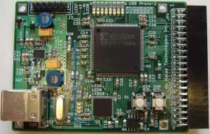
FPGA Board
FPGA Architecture Design Flow
FPGA Architecture design comprises of design entry, design synthesis, design implementation, device programming and design verification.
Design verification includes functional verification and timing verification that takes place at the time of design flow. The following flow shows the design process of the FPGA.
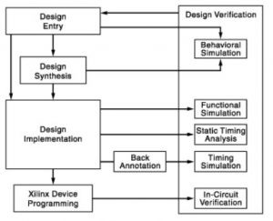
FPGA Architecture Design Flow
Design Entry
The design entry is done in different techniques like schematic based, hardware description language (HDL) and a combination of both etc. If the designer wants to deal with hardware, then the schematic entry is a good choice.
If the designer thinks the design in an algorithmic way, then the HDL is the better choice. The schematic based entry gives the designer a greater visibility and control over the hardware.
Design Synthesis
This process translates VHDL code into a device netlist format, i.e., a complete circuit with logical elements. The design synthesis process will check the code syntax and analyze the hierarchy of the design architecture.
This ensures the design optimized for the design architecture. The netlist is saved as Native Generic Circuit (NGC) file.
Design Implementation
The implementation process consists of
- Translate
- Map
- Place and Route
Translate
This process combines all the input netlists to the logic design file which is saved as NGD (Native Generic Database) file. Here the ports are assigned to the physical elements like pins, switches in the design. This is stored in a file called User Constraints File (UCF).
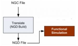
Translate
Map
Mapping divides the circuit into sub-blocks such that they can be fit into the FPGA logic blocks. Thus this process fits the logic defined by NGD into the combinational Logic Blocks, Input-Output Blocks and then generates an NCD file, which represents the design mapped to the components of FPGA.
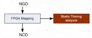
Map
Routing
The routing process places the sub-blocks from the mapping process into the logic block according to the constraints and then connects the logic blocks.
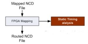
Routing
Device Programming
The routed design must be loaded into the FPGA. This design must be converted into a format supported by the FPGA. The routed NCD file is given to the BITGEN program, which generates the BIT file. This BIT file is configured to the FPGA.
Design Verification
Verification can be done at various stages of the process.
1.Behavioral Simulation (RTL Simulation)
Behavioral simulation is the first of all the steps that occur in the hierarchy of the design. This is performed before cheap lace dresses the synthesis process to verify the RTL code.
In this process, the signals and variables are observed and further, the procedures and functions are traced and breakpoints are set.
2. Functional Simulation
Functional simulation is performed post-translation simulation. It gives the information about the logical operation of the circuit.
3. Static Timing Simulation
This is done post mapping. Post map timing report gives the signal path delays. After place and route, timing report takes the timing delay information. This provides a complete timing summary of the design.
Applications of FPGA
- FPGAs have gained a quick acceptance over the past decades. Here are the some of the applications of FPGAs in various technologies.
- Users can apply them to the wide range of applications like random logics, SPLDs, device controllers, communication encoding and filtering.
- The emulation of entire large hardware systems via the use of many interconnected FPGAs.
- They offer a powerful solution for meeting machine vision, industrial networking, motor control and video surveillance.
- FPGAs are used in custom computing machines.
- FPGAs provide a unique combination of highly parallel custom computation and low-cost computation.
This is all about FPGA architecture. FPGA provides a new generation in the programmable logic devices.
The word Field in the name itself denotes to the ability of the gate arrays to be programmed for a specific function by the user instead of by the manufacturer of the device. The word Array is used to denote a series of columns and rows of gates that can be programmed by the end user.
Furthermore, any queries regarding this concept or electrical and electronic projects, please give your feedback in the comment section below. Here is a question for you, what are the three major components of FPGA Architecture?