Before clearly knowing about the tool EasyEDA, let us first understand why this tool is required and how it saves cost and time in the domain of electrical engineering. People who work in the professions of the embedded engineer, electrical engineer, and electrical tester, have to design circuits, create boards and simulate the boards in an easier and simpler approach. So, EasyEDA is the online tool that crucially helps in the design of circuits. The initial version of this tool was appeared in the year August 2013, whereas the official launch took place in March 2014. The final version which is currently in use has built quickly with multiple major revisions and improvements. The people who are behind the invention of this tool were Dillon He and Eric Cuit. Today, let us know what is EasyEDA and how to design circuits online free with EasyEDA?
What is EasyEDA?
EasyEDA corresponds to Easy Electronics Design Automation. The name itself indicates that it is easy to design circuits. This is the web-based tool package that allows embedded, hardware, and electrical engineers, and many others to design a circuit, simulate, share and look into the circuit’s schematics, printed circuit boards, and simulations through this comprehensive tool. Integrated with LCSC components and JLCPCB PCB service, the tool allows users in turning their ideas into reality.
The title of the article itself mentions that is freely available software where any can use this tool without purchasing. Go with the process of registration and login and a person is ready to create their own circuits. The supported operating systems and browsers are (Windows, Mac, and Linux) and (Chrome, Internet Explorer, Safari, and Firefox). After designing the project, there is no chance of missing the project because it will be saved on the EasyEDA website itself.
Features
Assimilated with multiple features, this tool stands as the best and most utilized circuit development tool for many. A few of the basics/features of EasyEDA are:
- Shows easier and efficient capabilities in circuit designing
- Sharing – publicly and privately
- Can develop numerous open-source projects
- Supports script and provides API
- Embedded with components purchase and PCB fabrication features
- Online sharing of projects
- Setting of themes
- Recovery of documents at any level
- Exporting documents in PDF, SVG, and PNG forms
- Export of Netlist such as FreePCB, Spice, Pads, and Altium Designer
- Design rules checking
- BOM/DXF exports
- PCB module
- Access to nearly 10,00,000 public libraries
- Management of various libraries
- Creating and editing symbol/Subpart and Spice symbol/model
- Footprint creation and editing
Step-by-Step Designing
- Open the editor section in the tool
- Select either components/footprints to be created
- Create new components
- Create new footprints
- Schematic capture
- Verify the circuits through simulation procedure
- Run simulation
- Conversion of Schematic Layout to PCB
- Ordering PCBs
EasyEDA supplies PCBs directly, or one can download the Gerber files and choose other suppliers to provide PCBs.
Getting Started with EasyEDA
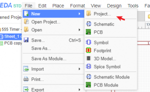
Open the EDA official website and create your account in this online circuit simulator tool. The tool shows the option either to create your own account or use the tool by logging through QQ or Google accounts. Now, provide the Gmail details and login to the website. Start creating your circuit design by choosing the “New Project” option.
Board Design with EasyEDA
Before placing the footprints, a board outline has to be created. In the board outline layer, draw the outline and this acts as the active layer. Using the options Arc and Track from the PCB tools palette, draw the outline. While the conversion of the schematic to PCB, the tool tries to create a board for you. In general, the default board outline area is almost 1.5 times more than the total area of all the footprints.
This means that total footprints can be placed in this outline providing space for tracking too. The board can be customized in your way by removing the elements. In order to create a basic rectangular board, the arc can be removed and lines are dragged from the “Properties’ panel.
The tool directly provides the options of Circular, Rounded rectangular, and rectangular board outlines. But for designing more complicated board outlines, a DXF file has to be imported.
Schematic Designing
In order to develop a printed circuit board, initially, a schematic plan of the circuit has to be prepared. Planning a schematic will help as a blueprint for placing the traces and setting all the components on the PCB board. In addition, the PCB software can also have the ability to import all the footprints, wires, and components onto the PCB file and the entire process allows the easy designing of the circuit.
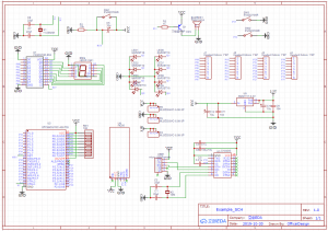
Start creating the schematic layout of the circuit by clicking on the “New schematic” option. Now, select all the desired components from the libraries section. Otherwise, search for the required component by clicking on ‘More Libraries’ and select the component. Drag all the required components from the left panel into the empty canvas section. Either right-click or press the ESC button to exit after placing all the components. Establish wiring between the components just by dragging the wire between components. When the properties or attributes of the component gas to be changed, click on the specific component, and modify from the right-side panel section.
After drawing the schematic, save it under your project and then proceed with the simulation process.
This is how drawing the schematic using EasyEDA tool can be done.
Simulating the Circuit in EasyEDA
Once the schematic layout of the circuit is completed, click the green button which is at the top bar and this runs the simulation. In the next pop-up window, select the type of simulation to run and proceed with running the simulation by clicking on ‘Run’.
There are five types of simulation which are
- Transient
- Ac analysis
- DC sweep
- DC transfer
- DC op pnt
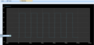
Let us consider that we are using a transient type of simulation for designing the inverter circuit. Here we will be considering AC output delivered from the inverter is driven to run home applications. For this process to take place, the inverter circuit should function at 50Hz frequency. For this considerable START and STOP, time periods are to be chosen for easy understanding of the simulation graph.
After the simulation is done, the graph can be viewed at the selected terminal. This terminal has to be chosen by keeping the end of the probe at the selected point. The below figure shows how to see the graph at the desired point by choosing the probe. The waveforms are like below which can be saved and download in multiple formats like JPG, PDF, PNG, and others.
PCB optimization
While proceeding with PCB conversion, it is required to know about few terms in the circuit designing which are of:
User Interfaces
Placing the components such as power connection, audio cords, potentiometers, LED displays shows the impact on the design of PCB.
PCB Layers
When there is the requirement to design complicated circuits, it is somewhat complex to design on a single layer because there is difficulty in tracing the routes without intersection with other components. For this, it is better to utilize two copper layers that have traces on both sides of the board. With the option ‘via’, the traces on both sides of the board can be connected. Via represents a copper-plated hole in the board that establishes the connection between the layers.
Ground Layers
For a few double-layered PCBs, there will be a ground layer where the complete bottom layer is coated with the copper plane that has a connection with the ground. The positive traces are channeled at the top position and the connections are grounded using holes or vias. Ground layers are helpful for circuits in eliminating interference problems and to dissipate the heat released by the components.
The thickness of the Layers
In general, copper weight defines the thickness of the layer which is calculated in ounces. The layer thickness shows the impact on the amount of current flow across the circuit and showing no damage to traces. Also, trace width is the other parameter that describes the amount of current that safely flows across the circuit. To find out the trace thickness and width measurements, an online trace width calculator helps a lot.
PCB Traces
For many of the copper traces, it can be observed that they bend at an angle of 450. The angle is of 450 because it reduces the electrical path in between the components. The other foremost reason is that elevated speed logic signals might be reflected off the back of the angle which causes interference.
When digital logics or else high-speed communication protocols that are more than 200 MHz are implemented in the project, then the best-used angle level has to be 450. Also, in the case of minimal speed circuits, 900 angles are not used where this angle level reduces the circuit’s performance.
Trace Width
Similar to the thickness of the layer, trace width also shows the impact on the amount of current flow across the circuit showing no harm to the circuit. The vicinity of traces for components and nearby traces defines the trace width.
Project to PCB Conversion
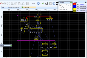
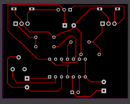
For converting the project to PCB, in the schematic board click on the option “PROJECT to PCB”. It directs you to the PCB designing board. If any of the components in the schematic diagram has no PCB traces, it notifies to select the proper component and proceed. Select the component depending on the view and click on ‘Submit’. Now, in the PCB design board, entire components will get distributed as per the PCB model board which is shown in the below picture.
Organize all the components in a systematic manner. Once the arrangement of the components is completed, the input will be at one terminal and the output will be at another terminal. Locate the light blue colored lines on the PCB board without interrupting the other. Do many required loops as you desire. Make sure that the traces should not be close to each other. After the completion of tracing, proceed with printing of the PCB board.
For this, click the ‘Print’ option which is in the file menu. Print the required layer by choosing the option. When there is only one layer, the created configuration can be printed as it is. The design can be printed either on glossy kind of paper for PCB engraving or provided to other suppliers.
This is the procedure of PCB layout conversion using EasyEDA.
PCB Ordering Process
This online PCB design tool also provides the option of ordering PCBs. For this click the ‘Fabrication Output’ button which is at the top menu in the PCB editor. In the next screen, the tool shows the options for ordering PCB like PCB dimensions, color, thickness, surface finishing, the required number of layers, and others.
Once the selections are finalized, click the option ‘Save to Cart’ and you will be directed to the next page for entering billing details. Furthermore, there is the option of downloading Gerber files in case you desire to purchase the board from other manufacturers. Gerber files correspond to a set of image documents to be provided to the manufacturer and these are compressed into a zip file.
Please refer to this link to know more about PCB Design MCQs.
So, designing our own printed circuit board lets us know what the exact results can be. And this article has explained clearly PCB designing, schematic diagram drawing, PCB layout conversion, and simulating the circuit. Also, know more about how this online circuit simulator helps for designing more complicated circuits and applications of EasyEDA?
