A JFET or Junction Field Effect Transistor is a transistor that classified under the category of FET. These are known for its voltage-controlled transistors where it doesn’t depend on the current for biasing. These consist of source, gate and drain as its terminals. This transistor comes under unipolar devices. The reason for this is that the conduction is dependent on the majority of the charge carriers. These FETs has the capability of consuming lesser amounts of power. It can be manufactured in the compressed and the much smaller sizes in comparison with the BJT. So it can be a great replacement when these points are a major concern. Even JFET is the extension of the FET.
Like BJT ,the FETs also consists of three terminals and in between the terminals, the channels are present for conduction. The FET has many advantages over BJT and the major one is the high impedance value at the input.
What is a Junction Field Effect Transistor?
JFET is a Junction Field Effect Transistor that is formed by the diodes with the junction of P-N. The conduction in the FET because of the type of channel formed between the terminals defines the JFET.
The JFET is classified as
(1) N-Channel JFET

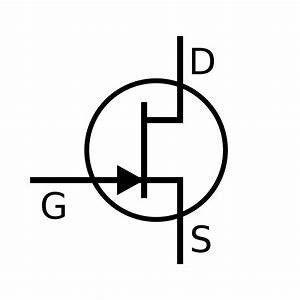
Symbol of N-Channel JFET
(2) P-Channel JFET

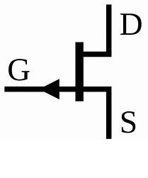
Symbol for P-Channel JFET
These are the symbols that define the difference in their functionalities based on their arrow indication. The arrow indication determines the flow of current when the gate and source terminal is forward biased.
N-channel JFET
A channel is responsible for the conduction in JFET when a voltage is applied between the terminals of the source and the drain. If the channel is of n-type then it is referred to as N-Channel JFET.
This channel consists of the doping concentration of the impurities type of donor indicating that the majority of the negative charges flow through it. Hence the majority of the concentration of carriers here in this channel is of type electrons.
JFET Working (N-Channel)
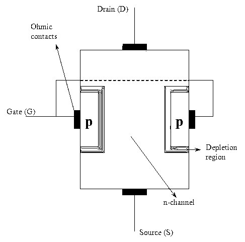
In this JFET on end of the n-channel is connected through a ohmic contact to the drain terminal and another end is connected to the source terminal. The two p type material is connected to the gate terminal. When the drain to source terminal is forward biased with the external supply the conduction begins. Due to the biasing a two pn junction becomes reverse biased near the drain and source terminal.
The region of the source is powered with a lower value of the potential than the drain due to this the region of depletion is more at the drain terminal compared to the source terminal. As the potential is increased, the width of the region of depletion at the junctions tends to increase.

N-Channel JFET Representation
This is the major reason due to which the flow of the majority concentration of carriers can be evident from the terminal drain to the lower potential applied terminal called source. These majority charge carriers flow is noted in a linear manner. As the value of the differences in potential increases between the terminals of drain and the source, the flow of the currents tends to be in continuous.
But the at a particular voltage at the drain and the source, the transistor reaches the condition of voltage known as the pinch-off voltage. Here current flow reaches the saturation level at the transistor. In this case, the transistor is referred to as the resistor that is controlled by the voltage.
Modes of FETs
As the voltages applied to the input terminal decides the various modes of the FET.
(1) Ohmic Region
The region at which the current value of the drain behaves linearly to the applied voltage as input at the drain and the source terminal is referred to as the Ohmic Region of field-effect transistor. In this case, the FET acts like a resistor that is controlled by the voltage.
(2) Pinch-OFF Region
The resistance value at the channel present between the terminals of the source and the drain is at peak during this region. Theoritically there should be no evident flow of the current at the pinch off condition. But when the gate to source terminal is zero the drain current reaches the saturation level.
(3) Saturation Region
In this region, the behavior of the transistor turns as the conductor. The current at the drain gets controlled by the amount of the voltage applied at the terminals of the source and gate. Where the voltage value at the drain and the source don’t get affected but at this region, the maximum value of the current flows from the terminals of drain towards the source. This region in FET is also referred to as Active Region. Hence the FET is considered to be fully ON at this region.
(4) Breakdown Region
As the value of the voltage applied between the terminals of the drain and the source is considered to be high due to this the current value at the drain tends to increase drastically. Hence the channel at the drain and the terminal source gets affected resulting in the breakdown condition. The device should not be operated under this condition. These voltage values are generally specified in the data sheet.
Hence the above discussed are the operating modes involved in the field-effect transistor.
JFET Characteristics
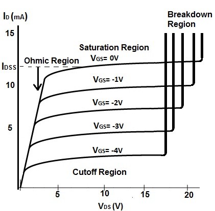
The curves plotted in between the current value at the drain and the voltage applied in between drain and the source by considering the voltage at the gate and the source as the parameter decides the characteristics of output that are also referred to as the drain characteristics.

N-Channel JFET Characteristics
Drain Characteristics of Junction Field Effect Transistor(JFET)
The drain characteristics of the JFET are
- When the positive voltage is applied to the drain to source terminal of JFET and when the gate to source voltage is zero, the Drain current starts flowing and the device is said to be in ohmic region.
- As the drain voltage is increased the channel of conductance tends to become narrower and narrower and current at the drain terminal gets smaller .
- At a particular drain to source voltage called the pinch-off voltage the drain current reaches the saturation level.
- Now if a negative voltage is applied to the gate terminal then, in that case, the channel present at the gate is reverse biased and the saturation current starts decreasing further. At a particular gate voltage the device stops conduction this is called the cut-off-voltage.
- But if the drain to source voltage is increased further then the device reaches the breakdown region in which the drain current increases indefinitely.
Please refer to this for How to Select a Transistor.
Please refer to this link to know more about Filed Effect Transistor
In this way, the various modes, as well as the region which determines the characteristics of FET, are discussed. Can you tell which can be preferred n-channel or p-channel for various amplification or switching applications?