A Hex inverter IC is a type of chip that includes six inverters within a single package. So, every inverter in this IC has a single input and output which performs the logical inversion operation. This IC is used for signal inversion, conversion of logic level & CLK signal generation within digital electronics. These inverter ICs are found easily in most electronic devices that produce data in small circuits. Examples of hex inverter ICs are CD4069 IC, M74HC04, and 74HCT04. So, this article discusses an overview of CD4069 IC, pinout, specifications, circuit, working, and its applications.
What is CD4069 IC?
The CD4069 IC is a CMOS hex inverter chip that is available in 14 14-pin DIP package. It is used in all general-purpose inverter applications wherever logic level and medium power TTL drive conversion capabilities of circuits are not necessary like CD4009, CD4049 hex inverter & buffers. So this IC is made up of six inverter circuits & complementary CMOS technology to provide low power consumption, fall timings, wide operating range, symmetric controlled rise, and good noise immunity.
CD4069 IC is suitable for mainly medium-speed applications when the propagation delay time at 10V is 30ns & it will rise when the voltage level goes down. So its max Input current over its working temperature range is 10mA and its maximum input voltage is 15Volts. This IC has 0.45V high noise immunity.
CD4069 IC Pin Configuration:
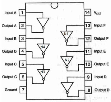
The pin configuration of CD4069 IC is shown below. This IC includes 14 pins which are discussed below.

CD4069 IC Pin Configuration
- Pins A, B, C, D, E & F (1, 3, 5, 9, 11 & 13): These are input pins of the inverter IC.
- Pins A’, B’, C’, D’, E’ and F’ (2, 4, 6, 8, 10 & 12): These are output pins of the inverter IC.
- Pin-14 (VDD): This is a power supply voltage pin that operates from +3 to +15V range.
- Pin-7 (GND): It is a ground pin.
Features & Specifications:
The features and specifications of CD4069 IC include the following.
- CD4069 IC is a 14-pin hex inverter chip.
- It is available in the DIP package.
- Its operating voltage ranges from 3V to 18V.
- It has less power consumption.
- It has high operation speed and high noise immunity.
- It has a high output current ability.
- This IC has standardized symmetrical o/p characteristics.
- It includes 6-channels.
- The type of output is Push-Pull.
- The data rate is 24.
- The input type is standard CMOS.
- Its max IOL and IOH in mA are 6.8 and -6.8.
- Its operating temperature ranges from -55°C to 125°C
- Its input current maximum at 18V is 1 µA above the full package-temperature range at 18 V is 100 nA & 25°C
- Typical medium-speed operation like tPHL and tPLH at 10 V is 30 ns.
- It has high noise immunity typically 0.45 VDD.
Equivalent & Alternatives
Equivalent CD4069 ICs are; IC-74HCT04, CD4069UB, MM74C901, MM74C907, CD4049A, MM74C14 or MM74C914. Alternative CD4069 ICs are; CD4009 & CD4049.
Broken Wire Detector Circuit with CD4069 IC
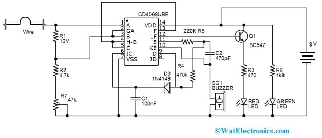
A broken wire detector circuit using CD4069 IC is shown below. So this circuit is used to detect the broken wire within the wall or some other place. By using this simple circuit, the precise broken wire location can be identified & the EMF (electromagnetic field) produced by the AC-carrying wire can be noticed. Whenever the break takes place, then this simple circuit provides a sound.
The required components to make this broken wire circuit mainly include; CD4069 IC, 20KΩ variable resistor, 1.2K, 10K, 220K, 330Ω, 470K & 1M resistors, 470pF & 100nF capacitors, 1N4007 diode, 9V battery, LEDs, BC547 transistor, and 5V Buzzer. Thus, connect this circuit as per the simple diagram shown below.

Broken Wire Detector Circuit with CD4069 IC
Working
This circuit can be designed with CD4069 IC which includes six CMOS inverters. This chip may be used for all general inverter applications. So this circuit is used mainly for up to 1KHz frequency oscillation.
In the above circuit, R3, R4 resistors & C2 capacitors help in oscillating the IC signals which are provided to the buzzer element, so it becomes enabled when the EMF detection on testing wire and two LEDs are connected through pin 12 of the IC through BC547 transistor. So, the Q1 transistor in the circuit works as a switch & makes the first LED glow throughout EMF detection then makes the second LED glow in the EMF absence.
This broken wire detector circuit must be used with perfect 15 cm wire with spiral wire length & it works as an EMF detecting antenna. So, this circuit sensitivity can be adjusted by the VR1 variable resistor. This antenna wire should not touch a high AC supply directly, so you must be secure while AC supply testing & do not touch any supply wire with bare hands.
Thus, this circuit is used mainly to verify wires in the walls that have been disconnected or broken. It detects broken wire like the AC voltage within the wire is detected.
Advantages and Disadvantages
The advantages of CD4069 IC include the following.
- The CD4069 hex inverter integrated circuit (IC) has many advantages, including:
- CD4069 IC has less power consumption, high current drive capability, and high noise immunity.
- This IC operates over a broad range of power supplies.
- It has consistent symmetrical output characteristics.
- This chip has a diode that clamps to defend all inputs from harm because of static discharge.
- It has of 35 ns propagation delay.
The disadvantages of CD4069 IC include the following.
- CD4069 ICs operation is slow.
- It has a lower packing density as compared to NMOS.
- These are expensive when processing steps are enhanced.
- These chips can be damaged through static charges above the leads but it can be avoided by in-built protective circuits or devices.
- These ICs can have power handling issues.
- These can be difficult to design.
Applications
The applications of CD4069 IC include the following.
- The CD4069 IC converts a lower voltage signal to a high voltage signal which is helpful whenever interfacing components that work at various voltage levels.
- This IC is used in general-purpose inverter applications wherever medium-power TTL drive & logic-level-conversion abilities are not necessary.
- It can be utilized for logic inversion, pulse shaping, and oscillators.
- This can be used mainly for high-input impedance amplifiers or logic circuits like; flip-flops, counters & oscillators.
Please refer to this link for the CD4069 IC Datasheet.
Thus, this is an overview of what CD4069 IC, pinout, features, specifications, circuit, working, and its applications. Here is a question for you, what is CMOS?