The transistor is a three-terminal semiconductor electronic device, used as a switch or an amplifier. Generally, transistors can be available in either PNP/NPN polarity with different switching and power speed ratings. If a transistor handles >1 Amps of collector current, then it is considered generally as a power transistor. These transistors must have less output resistance to deliver huge load currents and good junction insulation to oppose high voltages. These transistors can also dissipate heat very rapidly to avoid overheating. This article discusses an overview of the BD242 transistor, pinout, specifications, and its applications.
What is the BD242 Transistor?
BD242 is a PNP-type epitaxial silicon power transistor, available in a TO-220 leaded plastic package. It is mainly designed to be used in amplifier and switching applications and also series & shunt regulators. These transistors are also available in four different voltage ratings thus you can choose it based on your load requirements.
The absolute maximum collector-emitter voltage is around -45Volts, the collector-base voltage maximum is -55Volts, the emitter-base voltage maximum is -5V & maximum power dissipation is around 40W. This transistor is designed to be utilized in switching and amplification applications.
While looking for a suitable transistor for your application based on a few factors, it is very important to look into a few points on How to Select a Transistor.
Working
The BD242 is a general-purpose PNP-type transistor that is made up of an N-type material and is sandwiched among two P-type materials. The majority of charge carriers of this type of transistor are holes which are emitted by the emitter and collected by the collector. The flow of electrons in this transistor is from the emitter terminal to the collector. This transistor switches ON whenever there is a 0V or low voltage on the base terminal of the transistor. So it turns on whenever a small amount of current supplies throughout the collector terminal to the emitter.
Pin Configuration:
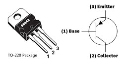
The pin configuration of the BD242 transistor is shown which includes three terminals like emitter, a base, and a collector which are discussed below.

BD242 Transistor Pin Configuration
- Pin-1 (Base): The base terminal helps in biasing the transistor. It transmits all the charge carriers without or with minimum loss from the emitter terminal to the collector
- Pin-2 (Collector): This terminal gathers all the charge carriers from the emitter terminal.
- Pin-3 (Emitter): This terminal emits all the free charge carriers into the primary PN junction.
Features and Specifications:
The features and specifications of the BD242 transistor include the following.
- BD242 is a PNP transistor.
- It is available in the TO-220 package.
- The transistor material is Si.
- Its maximum collector current or IC is -3Amps.
- Collector to emitter voltage maximum or VCEO is -45V.
- The collector-to-base voltage or VCBO maximum is -55V.
- The emitter to base voltage or VEBO maximum is -5V.
- Collector power dissipation or PC maximum is 40W.
- The emitter to base voltage maximum or |Veb| is 5 V.
- DC gain minimum or hFE is 25 at IC= -1.0Amps.
- Maximum operating and storage temperature must be -65 to +150 degrees Centigrade.
- The collector-emitter sustaining voltage or VCEO (SUS) minimum is -100V.
Equivalent & Complementary Transistors
Equivalent and replacement BD242 transistors are; TIP105, NTE153, TIP106, TIP126, TIP125, TIP135, BD202, TIP136, BD244, BD204, BD302, BD534, BD538, BD536, BD544B, BD648, BD644, BD796, BD800, BD896, BD810, BD900, BD898, BD934, BD938, BD936, BD948, BDT60, BD952, BD950, BDT64, BDT62, BDT82, 2SA1931, BDT84, 2SA614, 2SA489, 2SA671, 2SA614O, 2SA770, 2SA768, 2SB1015, 2SB1018, 2SB1017, 2SB1019, 2SB1097, 2SB1133, 2SB1024, 2SB1134, 2SB1136, 2SB1135, 2SB1187, 2SB1250, 2SB1223, 2SB1224, 2SB1225, 2SB1274, 2SB1251, 2SB1299, 2SB1368, 2SB1366, 2SB1375, 2SB1548, 2SB1565 and 2SB1566. A complementary BD242 transistor is a BD241 NPN transistor.
Replacing a suitable transistor in any circuit based on requirement is very important. To know how to replace it, please refer to this; Replacing Transistors in Electronic Circuits: Factors and Considerations.
How to use BD242 Transistor safely in a Circuit for a Long Time?
To keep it BD242 transistor very safely in a circuit for a long time, it is recommended to not connect this transistor wrongly and check its pin out always. It should not be used to its maximum ratings & stay always below 20% from the highest ratings. This transistor should not be connected to an above 36V load & do not drive any load > 2.4A. Additionally do not expose this transistor to excessive low or high temperatures. So it must be operated and stored from -65°C to 150°C temperature range.
Power Amplifier Driven 8R/6.25Wats Loudspeaker
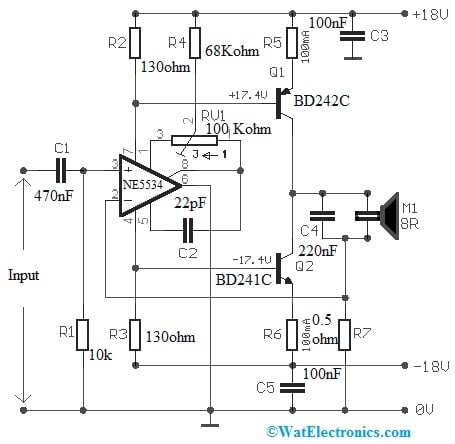
The power amplifier-driven 8R/6.25Wats loudspeaker circuit is shown below. This simple circuit was designed mainly for producing a power amplifier that can be used by loudspeakers through a 6.25W/8R rating. The required components to make this circuit mainly include; resistors; 10k, 130ohm, 68Kohm, 1ohm, 0.5ohm, capacitors; 470nF, 22pF, 100nF, 220nF, NE5534 IC, transistors like; BD242C, BD241C, 100 Kohm trimmer & 8Ohm>20W loudspeaker. Connect this circuit as per the diagram shown below.
The power amplifier is a kind of amplifier mainly designed for supplying and delivering adequate & highest high output power to drive loads or loudspeakers directly in a specified percent of distortion.
NE5534 is a low-noise and high-performance op-amp with combined and outstanding AC and DC characteristics. Its features mainly include; the capability of external compensation, offset nulling, broad voltage supply range, common mode rejection ratio-100 dB, less harmonic distortion at peak to peak with o/p voltage swing, higher slew rate, unity gain BW at 10 MHz, higher gain of DC voltage & equivalent input noise voltage.
BD242 transistor is a silicon epitaxial-base PNP type transistor that is used for high-speed switching and power amplifier applications including features like; 5Amps rated collector current, minimum 3 MHz frequency at 10V and 500 mA & 40Watts at 25°C case temperature.

Power Amplifier Driven 8R 6.25Wats Loudspeaker
Working
The amplifier in this circuit generates negative feedback where an actual signal is restricted by the fraction of the amplifier’s output that was united with the input. The load current does not depend on the loudspeaker’s impedance but instead on the input signal. So the current supply within the loudspeaker’s inductor generates a voltage because it merges with the R7 resistor. So this is the driving voltage to the op amp’s inverting input, which is accountable for generating the negative feedback. Here, the total voltage gain of the circuit mainly depends on the relation of the impedance of the loudspeaker to the R7 value.
NE5534 IC
Here, the NE5534 IC output connection in the ground is abnormal as the current supply from the Q1 transistor while the Q2 transistor is not driven by the NE5534 IC but through the supply lines. So the current is established through resistors & has from 50 mA to 100 mA value within the idle condition because it works in class-A mode.
The bias current in this class is greater as compared to the maximum output current which makes all o/p transistors continually conducting current. So it has low distortion & is the most linear type of amplifier.
Transistors
Here, Q1 and Q2 transistor operations must be matched to avoid the formation of large voltage & current differences. So the bias balancing can be attained by changing the R2 & R3 resistors to generate the current emitter of approximately 500 mA through Q1 & Q2 transistors. For the 8R & 6.25W kind of loudspeaker, the whole harmonic distortion is around 0.01% when being supplied through 18 V.
The power amplifiers in a transmission (or) output stage are used widely as the final stage amplifier that needs the most attention to power efficiency based on the classes utilized. Generally, some power amplifiers are flexible enough to drive a speaker within stereo mode using different impedance ratings which allows two separate amplifier circuits to produce high sound to a single channel. These amplifier applications mainly include; satellite communication, radio waves, biomedical engineering, hi-fi phonograph systems, deep sea telephone cables, electron tube creation, etc.
Connecting a base resistor to the base terminal of the transistor is mandatory to avoid it being damaged. So, please refer to this link for; Choosing Base Resistance for Transistors in Electronic Circuits.
Advantages & Disadvantages
The advantages of the BD242 transistor include the following.
- This transistor has a higher current ability.
- It has a low collector-to-emitter saturation voltage.
- It has a high DC gain and quick switching speed.
- This transistor has high current gain & less saturation voltage.
- It has less output resistance to deliver huge load currents.
- It has good junction insulation to oppose high voltages.
The disadvantages of the BD242 transistor include the following.
- This transistor is very sensitive to temperature.
- Transistors particularly in high-performance applications consume a significant amount of power that can lead to the generation of heat and reduced energy efficiency.
- It cannot be operated satisfactorily above the 15 kHz switching frequency.
- This transistor can be damaged because of the second breakdown or thermal runaway.
- It has a very low reverse-blocking capacity.
- Transistors in high-performance-based applications can use a significant amount of power thus it can lead to decreased energy efficiency & heat generation.
- The transistor fabrication process particularly at the nanoscale range needs expensive and highly complex manufacturing processes.
- Transistors can be vulnerable to a variety of reliability issues like; dielectric breakdown, hot carrier effects, and electromigration which can limit their lifespan and performance over time.
- These can be affected by sources of noise and electromagnetic interference, which degrades the performance and signal quality of electronic circuits.
BD242 Transistor Applications
The applications of the BD242 transistor include the following.
- BD242 transistor is mainly designed to be utilized in switching & amplification applications.
- This transistor is used in dimmers, inverter circuits, motor drivers, audio amplifiers, etc.
- This epitaxial silicon power transistor is used in battery charging and discharging circuits.
- It is used in different circuits like relay drivers, power converters, temperature control, DC to AC converters, power amplifiers, motor control, high voltage & high current-based switching circuits, LED drivers, and voltage regulation circuits.
- It is used in series & shunt regulators, switching & amplifier applications, Hi-Fi amplifier drivers & output stages.
- It is used in power supplies, audio amplifiers, high-power applications, and motor control circuits.
- It is apt for high-power switching applications due to high current gain and low saturation voltage.
Please refer to this link for the BD242 Transistor Datasheet.
Thus, this is an overview of the BD242 Transistor, pinout, features, specifications, circuit, working, and its applications. This is an epitaxial-based silicon-type NPN transistor that is mounted TO-220 plastic package. So these are intended to be used within medium power linear & switching applications. Here is a question for you, what is a BD241 transistor?