The BC107 is an NPN small-signal BJT available in different variants like; BC107A, BC107B, & BC107C where each has slightly special specifications. The main variation between these three variants is their hFE (current gain) range. So, BC107A transistor hFE ranges from 110 to 220, BC107B transistor has 200 to 450 ranges and BC107C transistor has 420 to 800 ranges. Based on the requirements of your application, a suitable variant is selected. This transistor is well-known in various circuit designs for its good performance and reliability. This article discusses an overview of the BC107 transistor, pinout, specifications, and its applications.
What is BC107 Transistor?
The BC107 is an NPN-type low-power bipolar junction transistor, available within a TO-18 metal case package. It is designed mainly for general-purpose switching & amplification purposes in electronic circuits like an amplifier, switches, and rectifiers. BC107 transistor gain is 50 which determines the ability to amplify this transistor. The highest current that can be supplied through the collector pin will be 100mA. The emitter & collector terminals of this transistor are left free whenever the base terminal is at the GND and after that it will be closed whenever a signal is provided to the base pin.
While looking for a suitable transistor for your application based on a few factors, it is very important to look into a few points on How to Select a Transistor.
Working
BC107 transistor is a current control device so whenever the small current supply on the base terminal is utilized to control the large amount of current on the remaining emitter and collector terminals. Whenever a voltage supply is provided to the base terminal, then it will be biased & draw current. After that control the large current supply on the both emitter & collector terminals.
The movement of charge carriers plays a key role in the transistor conductivity but the majority of charge carriers of this transistor are electrons. The electron’s free movement works like a bridge between the emitter & the collector terminals. The main function as well as doping concentration of the three terminals is not the same because the emitter terminal is highly doped as compared to the base & the collector terminals. The voltage supply on the collector terminal is much greater as compared to the base voltage.
Pin Configuration:
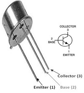
The pin configuration of the BC107 transistor is shown below. This transistor includes three terminals which are discussed below.

Pin Configuration
- Pin-1 (Emitter): This terminal is connected usually to the ground which handles the gate voltage drain of the transistor.
- Pin -2 (Base): The base terminal handles the transistor biasing by turning ON or OFF.
- Pin-3 (Collector): This terminal handles the current flow and is connected usually to the load.
Features and Specifications:
The features and specifications of the BC107 transistor include the following.
- BC107 is an NPN transistor.
- It comes in a TO-18 metal case package.
- The collector-to-emitter voltage of the transistor or VCEO is 45V.
- Its continuous current gain or HFE is 450.
- The base-to-emitter voltage of the transistor is 6V.
- The continuous collector current is 100mA.
- The collector-base voltage or VCBO is 50V
- The current gain or hFE maximum is 450.
- Its continuous collector current is 100mA.
- Its collector-to-emitter voltage or VCEO is 45Volts.
- The collector to base voltage or VCB0 is 50V.
- The emitter to base voltage or VBE0 is 6V.
Equivalent & Complementary Transistors
Equivalent BC107 transistors are: BC547, BC549, 2N3904, BC177, 2N706, 2N5581,2N2369, BCW65, D27Z, MPSL51,BCW65, BCW65 & MPSL51. The complementary BC107 transistors are BC177B and BC177 respectively.
Replacing a suitable transistor in any circuit based on requirement is very important. To know how to replace it, please refer to this; Replacing Transistors in Electronic Circuits: Factors and Considerations.
How to Utilize the BC107 Transistor Properly?
To use the BC107 transistor properly within your application, you need to know the transistor biasing and calculate the suitable resistor values for your particular application.
Transistor Biasing
Generally, transistor biasing involves setting the DC operating point to make sure of correct operation within the preferred region like active region, saturation, (or) cut-off. So the most frequently used biasing for this transistor is the common emitter, wherever the emitter terminal is connected simply to GND, and both the base & collector terminals’ voltages are set through resistors.
Resistor Values Calculation
To calculate the values of the resistor for transistor biasing, you need to think of the preferred collector current, the base current, and the voltage supply. So the below steps outline the procedure:
- Determine the necessary collector current based on the application requirement.
- Determine the base current with the current gain value of transistor IB = IC / hFE.
- Select an appropriate value mainly for the collector resistor depending on the voltage supply & the collector current like; RC = (VCC – VCE) / IC, wherever ‘VCE’ is the collector to emitter voltage.
- Calculate the base resistor value with the base current & the preferred base voltage like; RB = (VCC – VB)/IB.
Crystal Tester Circuit with BC107 Transistor
Generally, Crystal materials are expensive, so you cannot measure them with a normal multimeter. But, if you want to test whether it is bad or good, then the following simple crystal tester circuit is designed. Crystal helps in generating radio frequencies by working in clock signal controllers. In addition, these can be found in digital circuits and quartz watches. So this circuit tests crystals from the range 100 kHz – 900MHz.
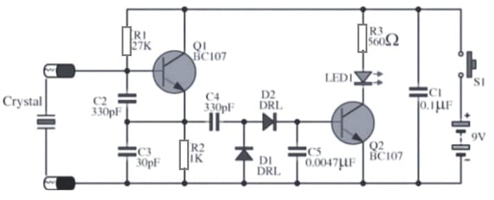
The required components to make this circuit mainly include; 9V battery, S1 switch, crystal, BC107 transistors, LED, D1 DRL, capacitors like; 330pF, 30pF,0.1uF, 0.0047uF and resistors like; 27K, 1K,560K. Connect the circuit as per the diagram shown below.

Crystal Tester Circuit with BC107 Transistor
Working
The BC107 transistor in the above circuit is a significant component and it generates a frequency whenever you situate a crystal on the connected socket to the base terminal of the transistor. Thus, whenever you push the switch, it allows the flow of current from the battery toward the circuit. In addition, it can also allow the generated oscillated signal from the Q1 transistor to move to the C4 capacitor. So, the oscillator signal constantly changes and the D1 & D2 smoothens the current.
The signal can also go throughout the C5 capacitor to smoothen the signal. So once this occurs, the positive voltage of C5 triggers a bias current that will supply to the Q2 transistor and turn ON LED1. Furthermore, the R3 resistor will restrict the current flow to the LED1 to prevent it from supplying 20mA from harming the LED. As a result, LED1 illuminates whenever Q1 works. Conversely, the Q1 transistor requires a quality crystal to build frequency. Thus, by using this, it is very simple to measure any crystal.
Connecting a base resistor to the base terminal of the transistor is mandatory to avoid it being damaged. Please refer to this link for; Choosing Base Resistance for Transistors in Electronic Circuits.
Voltage Doubler Circuit with BC107 Transistor & NE555 IC
An electronic multiplier circuit that is used to generate a DC output with double amplitude as compared to the AC input voltage amplitude is known as a voltage doubler. The voltage doubler circuit using BC107 & NE555 IC is shown below. This circuit utilizes the 555 timer IC, connected like a stable multivibrator for providing the input supply to the charge pump. To maintain excellent output voltage regulation, the load current must be low.
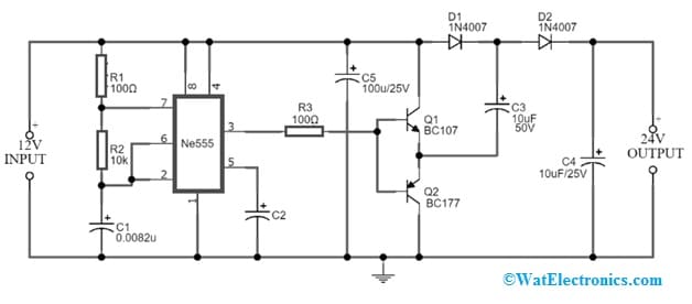
The required components to make this voltage doubler circuit mainly include; Resistors like; 10K and 100 ohms, NE555 Timer IC, capacitors like; 10uF, 0.0082uF and 100uF, 1N4007 diode, Transistors like; BC107 and BC1777 and 12V power supply. Connect the circuit as per the circuit shown below.

Voltage Doubler Circuit with BC107 & NE555 IC
Working
The voltage doubler circuit uses IC NE555 which works at 90KHz within a stable multivibrator mode. So both the transistors in this circuit like BC107 and BC1777 are together shorted. The output from the pin-3 of NE555 IC is provided to the transistor. So Q1 which is known as the lower output transistor will be turned OFF and the Q2 transistor will be turned ON. Whenever the IC output signal is high then the Q1 transistor will be turned ON & Q2 transistor will be turned OFF. So we can get the output twice to the input voltage. This simple circuit is used in radar devices, X-ray systems, etc.
How to use BC107 Transistor securely in a Circuit for a Long Time?
To ensure secure use and lasting performance in a circuit, it is suggested not to use at its maximum ratings. Always stay below 20% of its complete maximum ratings. So, the max collector current of this transistor is 100mAmps so do not drive any load > 80mAmps. The maximum CE voltage is around 45Volts so do not drive load > 36V. The collector terminal of this transistor is connected to the case thus it must be separated from the circuit connections (or) if the heat sink is utilized it must be isolated. The transistor must be utilized at above -65 °C & below 150°C temperature.
Precautions
Whenever the BC107 transistor is used in a circuit, the following tips & precautions need to be followed.
- Always make sure the transistor is correctly biased to function within the desired region.
- Do not go beyond the maximum ratings mentioned above to avoid damage.
- Utilize suitable heat sinking whenever the transistor is necessary to dissolve significant power.
- Be aware of the polarity of the transistor whenever it is connected within a circuit because wrong connections can lead to breakdown or injury.
- Utilize coupling capacitors whenever dealing with AC signals to avoid DC biasing issues.
- Consider the high-frequency limitations of transistors whenever designing high-frequency circuits.
BC107 Transistor Applications
The applications of BC107 Transistor include the following.
- It is used in Low noise circuitry, Darlington pairs, switching circuits, low noise signal processing, RF and Radio circuits.
- This transistor works in driver module applications like; relay drivers and LED drivers.
- This transistor is used to create a Darlington pair.
- It also functions within amplifier module applications like audio amplifiers and signal amplifiers.
- It can also used in consumer electronics, portable devices, etc,
- This transistor is used for industrial, power management applications, and signal processing applications.
Please refer to this link for the BC107 Transistor Datasheet.
Thus, this is an overview of the BC107 transistor, pinout, features, specifications, circuit, working, and applications. This is a low signal type NPN transistor and is well known for its low noise operations which make it suitable in television receivers and signal processing circuits. Here is a question for you, what is BC109 transistor?