A Darlington transistor is an electronic component that includes the combination of two PNP or NPN bipolar junction transistors which are connected back to back. The first transistor’s emitter terminal is connected to the second transistor’s base terminal. Therefore, the base supply is only provided to the primary transistor whereas the output current is received simply from the second transistor. So two transistors allow an extremely high amount of current gain. This can be achieved through compounding amplification, where the first transistor amplifies current and is further amplified through the second transistor. This Darlington transistor works as a single-unit transistor because it has one emitter, base, and collector only. This article provides an overview of the BD680 transistor, pinout, specifications, and applications.
What is a BD680 Transistor?
BD680 is a high gain and medium power PNP Darlington transistor which is available in the TO-126 package. This transistor is a three-layer device from the BD6xx series which can also include other transistors like; BD676A, BD676, BD678, BD680A, BD682 & BD678A. The transistor is designed to be used in general purpose amplification and switching purposes.
These Darlington transistors can also be utilized as output devices within complementary general-purpose amplifier-based applications. The collector current is a function of the base current, so a change within the base current provides a corresponding amplified change within the collector current for a specified collector-emitter voltage. When this transistor is used in any application, make sure always that appropriate heat sinking & consider the maximum ratings for voltage, current & power dissipation of the device to avoid injury and ensure reliable operation.
While looking for a suitable transistor for your application based on a few factors, it is very important to look into a few points on How to Select a Transistor.
Pin Configuration:
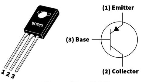
The pin configuration of the BD680 transistor is shown below. This transistor includes three terminals which are discussed below.

BD680 Transistor Pin Configuration
- Pin-1 (Emitter): This terminal is heavily doped and its main function is to supply charger carriers to the base terminal.
- Pin-2 (Collector): This terminal is slightly lightly less as compared to the emitter terminal. The collector junction gathers the majority of charge carriers which are emitted by the emitter.
- Pin-3 (Base): This is the middle region which is extremely thin and doped lightly. These terminals help in the biasing of the transistor.
Features & Specifications
The features and specifications of the BD680 transistor include the following.
- It is a three-terminal PNP-type Darlington transistor.
- This transistor is available in the TO-126 package.
- Its mounting style is Through a Hole.
- Configuration is single.
- It is electrically the same as the MJE702 transistor.
- Its maximum collector-to-emitter voltage is -80 Volts.
- The collector to base maximum voltage is -80 Volts.
- Its maximum emitter to base voltage is -5 Volts.
- Its max continuous collector current is -4 Amps.
- Collector dissipation is 40 Watts.
- DC’s current gain or hfe is 750.
- Its operating & storage junction temperature ranges from -65 to +150 °C
Equivalent and Complementary Transistors
Equivalent and Replacement of BD680 transistors are; 2N6036, BD680A, BD680AG, 2N6036G, BD680G, BD682G, BD682, BD780, KSE703, KSE702, MJE702G, MJE702, MJE703G or MJE703. The complementary transistors of BD680 are; the NPN BD679, BD675, BD677, BD675A, BD677A, BD679A, BD681 & BD679. The lead-free version of the BD680 transistor is BD680G.
Replacing a suitable transistor in any circuit based on requirement is very important. To know how to replace it, please refer to this; Replacing Transistors in Electronic Circuits: Factors and Considerations.
How to use BD680 Transistor Safely in a Circuit for a Long Time?
To use the BD680 transistor in a circuit for the long term, do not drive this transistor to its complete maximum ratings & stay at a minimum below 20% from its maximum ratings. Thus, the maximum collector terminal to emitter voltage must be -80V. So do not drive any load above -64V. Its maximum collector current must be -4A thus the derived load must be below 3.2Amps. In addition, the operating & storage temperature must be between -55°C to 150°Centigrade.
Discrete Voltage Regulator Circuit
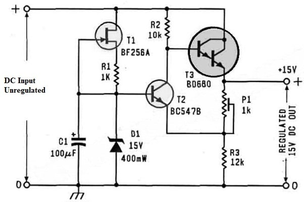
The discrete voltage regulator circuit is shown below which is a very simple & effective method to change as well as stabilize the o/p voltage within electronic circuits. This circuit uses a BD680 transistor which efficiently controls the voltage fluctuations to provide a constant power supply to a variety of components (or) loads.
The BD680 is a high-power transistor that handles up to 4A of current supply & this transistor has 80 volts of a max voltage rating. So this makes it appropriate for applications that need higher voltages & currents. Whenever this transistor is used in a discrete voltage regulator circuit, then it works as the main component that is accountable for voltage regulation.
This simple discrete voltage regulator circuit maintains a stable output voltage despite variations within the input voltage (or) variations within the load resistance. So this ensures that sensitive electronic components get a stable voltage by avoiding harm caused by voltage drops or spikes.
Required Components
The required components to make this circuit mainly include a few basic electronic components like; BD680, BF256A & BC547B transistors, 15V 400mW diode, 100uf Capacitor, 1k, 10k, 22k resistors, and 1k Potentiometer. Connect this circuit as per the circuit shown below.

Discrete Voltage Regulator Circuit Diagram
Working
In this circuit diagram, the output current ability can be determined by the o/p transistor using the BD680 transistor which delivers 4 Amps of a maximum current at 10 volts collector-emitter voltage to provide sufficient cooling. However, the 6A of peak current makes it challenging to equal through an incorporated voltage regulator.
The working of the discrete voltage regulator circuit itself is simple. The JFET T1 in the circuit ensures that the D1 Zener diode gets approximately 1 mAmps steady current which maintains a steady reference voltage.
To attain a steady startup, the C1 capacitor is connected simply with D1 in parallel. It provides extra buffering & reduces the noise & disturbances impact. So typically this circuit takes around a minimum of three seconds to completely start up.
Here an extra component like an output buffer is required to create a voltage regulator for the reference voltage. So this can be done throughout a super-Darlington configuration which includes T2 & T3 transistors. Even though this arrangement effectively works the main disadvantage is that the o/p voltage will be around one diode drop less as compared to the Zener voltage. So by integrating the P1 preset, this can be changed, but the o/p voltage will be somewhat lower as compared to the Zener voltage. This voltage can be modified with P1 preset (or) a wire bridge. So the maximum attainable output voltage is around 30 V.
Connecting a base resistor to the base terminal of the transistor is mandatory to avoid it being damaged. So, Please refer to this link for; Choosing Base Resistance for Transistors in Electronic Circuits.
BD680 Transistor Applications
The applications of the BD680 transistor include the following.
- BD680 is mainly designed for use in general-purpose switching & amplifier applications.
- This transistor can be used in audio amplifiers, switching circuits, motor control, DC-to-DC converters, power supplies, LED drivers, pulse generators, voltage inverters, voltage regulation, battery-operated devices, etc.
- These transistors can be utilized as output devices within general-purpose complementary amplifier applications.
- This transistor is used in medium-power linear applications.
- This PNP power transistor is frequently used in a variety of electronic circuits because of its robustness & high current handling ability.
- BD680 transistors are used in power supply circuits as current sources & sinks, linear voltage regulators, over-voltage protection circuits, etc.
- These are used in switching circuits as a switch within high current or high power applications.
- These are used in motor drivers & control circuits to handle stepper motors or DC motors.
- This transistor is used in battery charger circuits for voltage & current regulation.
- These are used in relay driver and inverter circuits
- This transistor is applicable wherever there is a requirement for a high-power and reliable transistor such as in automotive electronics, industrial control systems, or robotics.
Please refer to this link for the BD680 Transistor Datasheet.
Thus, this is an overview of the BD680 transistor, pinout, features, specifications, circuit, working & its applications. Here is a question for you, what is the BD679 transistor?
This is an epitaxial-base PNP silicon power transistor available in a monolithic Darlington configuration and mounted within the Jedec SOT-32 plastic package. These transistors are designed mainly to be used within medium power linear & switching applications.