Generally, BJTs are available in two types; PNP and NPN which have three pins, used mainly for external connections. As compared to PNP, the flow of current in the NPN transistor will be from the collector terminal to the emitter. Generally, transistors are known as current-controlled devices because they control the input current. In both the PNP & NPN transistor’s conductivity, charge carriers play a key role. So, the majority of charge carriers in the NPN transistor are electrons whereas holes in the PNP transistor. The conductivity within the transistor can be done by the electron’s movement which is very better as compared to the hole’s movement. This article provides brief information on one of the NPN transistors namely; the D882 transistor.
What is the D882 Transistor?
The D882 is a general purpose, medium power & high performance based NPN type transistor that is manufactured with planar technology. These transistors are rugged and high-performance-based transistors. This transistor can also be mounted on a heatsink within the SOT-32 package with a screw hole. The PNP-type complementary type of the D882 transistor is the 2SB772 transistor.
These transistors have some significant features; medium current carrying ability & high collector-emitter (CE) breakdown voltage. The amplification factor of this transistor is 60 to 400 which indicates the quantity of current this component can amplify. This transistor is perfect to utilize in a wide range of fields like hobbyists electronic projects, commercial and educational.
Working Principle
This D882 transistor action begins from the base terminal because this pin performs as a control valve to control the electron charge carriers that are emitting from the emitter. After that, they are gathered by the collector terminal. This collector terminal is connected through a resistor for controlling the flow of electrical current. Generally in the NPN transistor, the positive (+Ve) voltage supply is provided to the base terminal.
This transistor includes three layers, N P, and N. So the P-doped layer simply signifies the base terminal whereas the other two N-doped layers signify the emitter & collector where these two terminals are negative. Whenever a 5Volts supply is provided at the base terminal of this transistor then it gets biased & begins the transistor action. So the little i/p current is utilized to make a large o/p current at the remaining two terminals.
Pin Configuration:
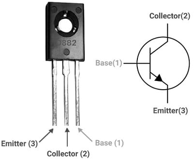
The pin configuration of the D882 transistor is shown below. This transistor includes three pins like BJT which are discussed below. The D882 transistor pin configuration with its symbol is shown below.

D882 Transistor Pin Configuration
- Pin1 (Base): The flow of current throughout this base terminal simply controls the conduction between emitter & collector terminals.
- Pin2 (Collector): This terminal allows the flow of current.
- Pin3 (Emitter): Current flows out from this terminal.
Features & Specifications:
The features and specifications of the D882 transistor include the following.
- The type of transistor is NPN.
- This transistor has three pins.
- The material of the transistor element is Silicon.
- Its contact plating is Tin.
- It is available to package or case is TO-225AA, TO-126-3
- Its height x length x width is 10.8mm x 7.8mm x 2.7mm.
- The type of mounting is Through Hole.
- It has less saturation voltage.
- The collector-to-emitter voltage (Vce) is 30V.
- The collector to base voltage (Vcb) is 40V.
- The emitter to base voltage (Veb) is 5V.
- The collector current (Ic) is 3A.
- The minimum saturation voltage at the collector is 0.3V only.
- Current gain (hfe) ranges from 60 to 400.
- Power dissipation (Ptot) is 10 watts.
- Its storage temperature (Tstg) ranges from -55 to 150C
- Its high current is 3A & voltage capability is 30V.
- Its maximum transition frequency or fT is 90 MHz.
- Its MSL (Moisture Sensitivity Level) is 1 (Unlimited).
- Alternative D882 transistors are; MJE802, BD131, BD185, BD349, MJE182, BD189, BD187, 2SC4342, TIP122L, 2SD1712, 2SD1018 & 2SD1693. The PNP complementary D882 transistor is 2SB772.
How to use a D882 Transistor safely in a Circuit for a Long Time?
To get good performance by using this D882 transistor it is recommended you should not drive any load above 3A. From the maximum load ratings, stay under 200mA always to be secure & utilize a suitable heatsink always. This transistor should not operate above 30Volts & use an appropriate base resistor always. Do not operate/store this transistor in the range of temperature under -55 degrees centigrade & above +150 degrees centigrade.
Audio Amplifier Circuit with D882 Transistor
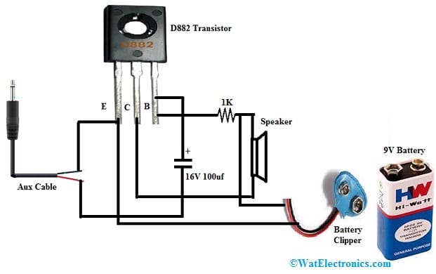
The simple audio amplifier circuit with D882 Transistor is shown below. The required components to make this simple amplifier circuit include; a 9V battery, D882 transistor, aux cable, battery clipper, 1K resistor, 16V 100uf capacitor & a speaker.
Connections
The connections of this circuit follow as;

Audio Amplifier Circuit with D882 Transistor
- First 1K resistor needs to connect to the transistor’s base terminal.
- A 16V 100uf capacitor’s positive pin is connected to the base of the transistor.
- Connect the aux cable to the circuit by soldering the +ve wire of the aux cable to the negative pin of the capacitor.
- Similarly, solder the negative wire of the aux cable to the transistor’s emitter pin.
- Connect the speaker’s +ve wire to the 1K Resistor & -ve wire to the collector pin of the transistor.
- Connect the battery clipper’s -ve wire to the emitter terminal of the transistor.
Working
This simple audio amplifier circuit with a D882 transistor works: for playing songs, need to connect the battery to the battery clipper & connect the aux cable to the phone. If you play any song, this amplifier will generate loud music sound as compared to a mobile phone. To get better quality sound from this amplifier, need to design a box for the speaker & situate the speaker on that.
Please refer to this link for Choosing Base Resistance for Transistors in Electronic Circuits.
Please refer to this link for Replacing Transistors in Electronic Circuits.
Please refer to this link for How to Select a Transistor.
Applications
The applications of the D882 transistor include the following.
- D882 transistor is generally used for switching & amplification purposes.
- The maximum collector current of this transistor like 3A is sufficient to drive several LEDs, relays, motors, Bulbs, etc.
- This transistor has 10W of max power dissipation so it is used for the audio amplifier’s o/p stages, bell circuits, and audio-based circuits.
- The D882 transistor is used for driving loads below 3A.
- It is used in H-bridge, power supply & voltage regulators.
- This transistor helps in driving motors & also battery charger circuits.
- It is used in voltage regulation, generic switches, relay drivers, DC-DC converters, audio amplifiers, Darlington pairs, etc.
Please refer to this link for the D882 Transistor Datasheet.
Thus, this is brief information on the D882 Transistor, pin configuration, features, specifications, circuit, working, and its applications. D882 transistor is a general-purpose, NPN transistor with high performance. This transistor comes under the NPN category in the TO-126 package. This transistor can be used in any load under 3A like battery charger circuits, power supply circuits, driving motors, etc. Here is a question for you, what is 2SB772 transistor?