PIC microcontroller is a programmable device that is used mostly in embedded systems, and also various engineering projects. There are various microcontroller families available like 8051, AVR, PIC, ARM, etc. Among them, PIC is one type of microcontroller family made by Microchip Technology. These microcontrollers are divided into four large families; PIC10, PIC12, PIC16 & PIC 17/18. The term ‘PIC’ stands for Peripheral Interface Controller and currently, it is developed as a Programmable Intelligent Computer. PIC devices are very famous with both hobbyists & industrial developers because of their low cost, large user base, wide availability, wide set of application notes, free development tools, and capability of re-programmable flash-memory & serial programming. This article provides brief information on the PIC18F4550 microcontroller.
What is the PIC18F4550 Microcontroller?
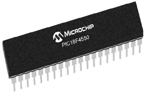
The PIC18F4550 microcontroller is from the PIC18F family and is one of the superior PIC microcontrollers from the microchip technology. This PIC microcontroller is very popular because of its functionalities with an integration of ADC & USB. These microcontrollers are available in different packages like QPF, QPN & DIP. This PIC microcontroller is a 40-pin and 8-bit microcontroller that has 32KB of Program Memory, 2048Bytes of RAM, 256Bytes of EEPROM Memory & 12MIPS of CPU Speed. This microcontroller comes with an Enhanced flash, High-Performance, USB Microcontroller through nano-watt technology.

PIC18F4550 Microcontroller
Features & Specifications:
The features and specifications of the PIC18F4550 microcontroller include the following.
- This microcontroller has 40 pins.
- PIC18F4550 microcontroller has an 8-bit CPU.
- Operating voltage ranges from +4.0 to +5.5 V.
- It has 35 I/O programmable pins.
- It has a programmable serial UART.
- It has a USB serial interface for communication.
- It has a 2-wire serial interface.
- It has a master or slave SPI serial interface.
- Timer module with one 8-bit counter and 16-bit counters -3.
- It has four PWM channels.
- This microcontroller has two analog comparators.
- It has a 32KHz to 8MHz calibrated internal oscillator.
- The external oscillator is up to 48MHz.
- It has 32Kabytes of program memory.
- The type of program memory is flash.
- It has 2K bytes of RAM.
- It has 256Bytes of EEPROM.
- Its operating temperature ranges from -40°C to +85°C.
- The speed of the CPU is 12 MIPS
- It has power-saving modes.
- It has a programmable watchdog timer with a separate On-chip oscillator.
- It has an ADC module with 13 channels and an ADC with a 10-bit resolution.
- Equivalent PIC18F4550 microcontrollers are; PIC18F4455, PIC18F2550 & PIC18F2455.
- PIC18F4550 Replacement is PIC18F4455 microcontroller and PIC18F4550 family microcontrollers are; PIC18F2550 and PIC18F2455.
Pin Configuration:
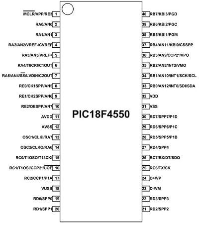
The pin configuration of the PIC18F4550 microcontroller is shown below. This microcontroller includes 40 pins and each pin and its functionality are discussed below.

Pin Configuration
Pin1 (MCLR/VPP/RE3): MCLR is a master clear pin, VPP is a programming input voltage and RE3 is an I/O pin of PORTE.
Pin2 (RA0/AN0): RA0 pin is PORTA’s I/O pin whereas AN0 is an analog input 0.
Pin3 (RA1/AN1): RA1 pin is PORTA’s I/O pin whereas AN1 is an analog input 1.
Pin4 (RA2/AN2/VREF-/CVREF): RA2 pin is an I/O pin of PORT-A, AN2 is an analog input-2, VREF is an A/D reference voltage i/p and CVREF is reference o/p of an analog comparator.
Pin5 (RA3/AN3/VREF+): RA3 is PORTA’s I/O pin, AN3 is analog input-3, VREF+ is an A/D reference voltage i/p.
Pin6 (RA4/T0CKI/C1OUT/RCV): RA4 is PORTA’s I/O pin, T0CKI is Timer-0 external CLK i/p, C1OUT is an output of comparator-1 and RCV is an external RCV i/p of USB transceiver.
Pin7 (RA5/AN4/SS/HLVDIN/C2OUT): RA5 is PORTA’s I/O pin, AN4 is an analog input-4, SS is slave select i/p pin of SPI, HLDVIN is high/low-voltage detect i/p and C2OUT is the output of the comparator-2.
Pin8 (RE0/AN5/CK1SPP): RE0 is an I/O pin of PORT-E, AN5 is analog i/p-5 and CK1SPP is o/p of SPP clock-1.
Pin9 (RE1/AN6/CK2SPP): RE1 is PORTE’s I/O pin, AN6 is an analog i/p-6 and CK1SPP is o/p of SPP clock-1.
Pin10 (RE2/AN7/OESPP): RE2 is PORTE’s I/O pin, AN6 is an analog input-7 and OESPP is enabled o/p of SPP.
Pin11 (VDD): It is a 5V power supply.
Pin12 (VSS): It is a Ground pin.
Pin13 (OSC1/CLKI): It is pin-1 of the oscillator and CLKI is an input of an external CLK source.
Pin14 (OSC2/CLKO/RA6): It is a pin-2 of the Oscillator, CLKO is an output of the clock source and RA6 is PORTA’s I/O pin.
Pin15 (RC0/T1OSO/T13CKI): RC0 is PORTC’s I/O pin, T1OSO is a Timer-1 oscillator o/p and T13CKI is Timer-1/Timer-3 external CLK i/p.
Pin16 (RC1/T1OSI/CCP2/UOE): RC1 is PORTC’s I/O pin, T1OSI is an oscillator’s Timer1 input, CCP2 is capture-2 input or comparator-2 o/p or output of PWM2 and UOE is an external USB transceiver OE o/p.
Pin17 (RC2/CCP1/P1A): RC2 is PORTC’s I/O pin, CCP1 is capture-1 i/p or comparator-1 o/p or output of PWM1 and P1A is an enhanced CCP1 PWM o/p.
Pin18 (VUSB): Output of internal USB 3.3V voltage regulator.
Pin19 (RD0/SPP0): RD0 is PORTD’s I/O pin and SPP0 is a streaming parallel port data.
Pin20 (RD1/SPP1): RD1 is PORTD’s I/O pin and SPP1 is streaming parallel port data.
Pin21 (RD2/SPP2): RD2 is PORTD’s I/O pin and SPP2 is streaming parallel port data.
Pin22 (RD3/SPP3): RD3 is PORTD’s I/O pin and SPP3 is streaming parallel port data.
Pin23 (RC4/D-/VM): RC4 is PORTC’s I/O pin, D- is a differential minus line of USB, and VM is VM i/p of external USB transceiver.
Pin24 (RC5/D+/VP): RC5 is PORTC’s I/O pin, D+ is a USB differential plus line and VP is the VP input of the external USB transceiver.
Pin25 (RC6/TX/CK): RC6 is PORTC’s I/O pin, TX is EUSART asynchronous transmit and CK is an EUSART synchronous CLK.
Pin26 (RC7/RX/DT/SDO): RC7 is PORTC’s I/O pin, RX is an EUSART asynchronous receive, DT is EUSART synchronous data and SDO is SPI data out.
Pin27 (RD4/SPP4): RD4 is PORTD’s I/O pin and SPP4 is streaming parallel port data.
Pin28 (RD5/SPP5/P1B): RD5 PORTD’s I/O pin, SPP5 is streaming parallel port data and P1B is a PWM o/p of enhanced CCP1 for channel-B.
Pin29 (RD6/SPP6/P1C): RD6 is PORTD’s I/O pin, SPP6 is streaming parallel port data P1C and PWM o/p of enhanced CCP1 for channel C.
Pin30 (RD7/SPP7/P1D): RD7 is PORTD’s I/O pin, SPP7 is streaming parallel port data and P1D is the PWM output of enhanced CCP1 for channel D.
Pin31 (VSS): It is a GND pin.
Pin32 (VDD): It is a 5V positive power supply.
Pin33 (RB0/AN12/INT0/FLT0/SDI/SDA): RB0 is PORTB’s I/O pin, AN12 is an analog i/p 12, INT0 is an external interrupt0, FLT0 is enhanced input of PWM Fault, SDI is a SPI data in and SDA is data I/O of I2C.
Pin34 (RB1/AN10/INT1/SCK/SCL): RB1 is PORTB’s I/O pin, AN10 is an analog input10, INT1 is an external interrupt1, SCK is synchronous serial CLK I/O for SPI mode and SCL is a synchronous serial CLK I/O for I2C mode.
Pin35 (RB2/AN8/INT2/VMO): RB2 is PORTB’s I/O pin, AN8 is an analog input-8, INT2 is an external interrupt-2 and VMO is an external USB transceiver output.
Pin36 (RB3/AN9/CCP2/VPO): RB3 is PORTB’s I/O pin, AN9 is an analog input-9, CCP2 is capture-2 input or compare-2 o/p or PWM2 o/p and VPO is an external USB transceiver o/p.
Pin37 (RB4/AN11/KBI0/CSSPP): RB4 is PORTB’s I/O pin, AN11 is analog input11, KBI0 is Interrupt-on-change pin and CSSPP is chip select control o/p of SPP.
Pin38 (RB5/KBI1/PGM): RB5 is PORTB’s I/O pin, KBI1 is an Interrupt-on-change pin and PGM is an enable pin of low voltage ICSP programming.
Pin39 (RB6/KBI2/PGC): RB6 is PORTB’s I/O pin, KBI2 is an Interrupt-on-change pin and PGC is the In-Circuit Debugger & CLK pin of ICSP programming.
Pin40 (RB7/KBI3/PGD): RB7 is PORTB’s I/O pin, KBI3 is an Interrupt-on-change pin and PGD is an In-Circuit Debugger & ICSP programming data pin.
PIC18F4550 Microcontroller Architecture
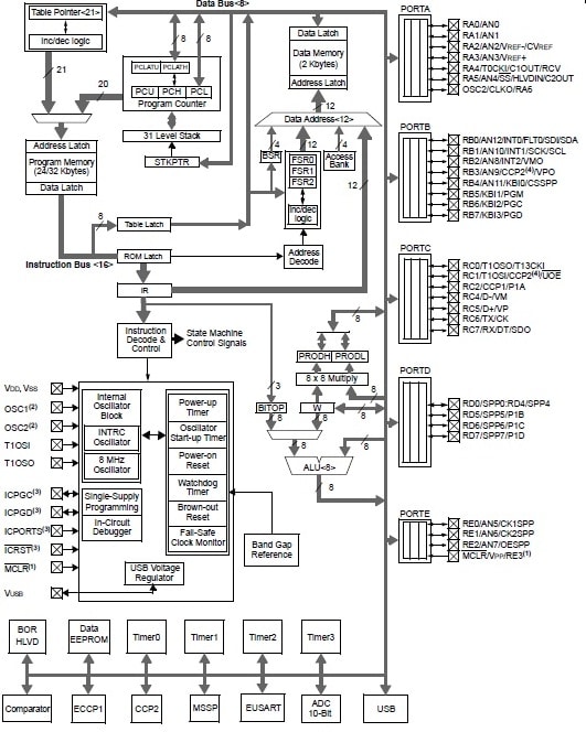
PIC18F4550 microcontroller is an 8-bit microcontroller from the PIC18 family. This family mainly depends on 16-bit instruction set architecture. PIC18F4550 microcontroller works on various internal & external clock sources. The frequency range of this microcontroller is from 31 KHz – 48 MHz. PIC18F4550 microcontroller has in-built peripherals like timers, comparators, ADC, etc. This microcontroller can also be equipped with superior communication protocols such as; EUSART, I2C, SPI, USB, etc.

PIC18F4550 Architecture
Ports
PIC18F4550 microcontroller includes five ports namely; Port-A, Port-B, Port-C, Port-D, and Port-E.
- Port A has a total of six pins which range from Pin-2 to Pin-7.
- Port B has a total of eight pins which range from Pin-33 to Pin-40.
- Port C has a total of eight pins but all these pins are not connected together. The first four pins are connected at Pin15 to Pin18 whereas the other four pins are connected at Pin23 to Pin26.
- Port D includes eight Pins which are also not connected together. So the first four Pins are connected at Pin19 to Pin22, whereas the other four pins are connected at Pin27 to Pin30.
- Port E includes three pins total which range from Pin8 to Pin10.
Registers
In the PIC18F4550 microcontroller, every port can be associated through three 8-bit registers for operations of IO like; TRISX (8-bit), LATx (8-bit), and PORTx (8-bit)
TRISx: In the TRISx register, the letter ‘X’ is the port name like TRISA, TRISB, etc. So this kind of register allocates the pins direction (Input / Output). For instance “TRISA = 0xF0”, sets all the pins within port A to o/p.
LATX: This register reads & changes the operation of write on the I/O pin value & stores the o/p data that is passed on to the external device.
PORTX: This register simply reads the level of the device, stores the pin input level, and reads and registers the i/p signal from the outside device if the pin is arranged as Input
Timers
The PIC18F4550 microcontroller has an inbuilt timer module that is used in many applications such as; Pulse counting, precise delay generation & measurement of pulse. The timers of this microcontroller are; Timer0, Timer1, Timer2 & Timer3. Timer1 is an 8-bit whereas Timer0 to Timer3 are 16-bit. These modules contain their individual Status and Control Registers. To utilize Timer like a counter otherwise to use for event counting, we have to connect the exterior pulse to RA4 mainly for Timer0 & RC0 mainly to Timer1. So these signals are T1CKI & T3CKI correspondingly.
ADC
This PIC microcontroller has 10-bit 13 channels analog to a digital converter where the channels are denoted with AN0 to AN12. ADC is mainly used for reading analog signals from different sensors & changing them into digital for further processing.
UART
UART in this microcontroller is used for communicating serially between two devices. Generally, the serial protocol is used for long-distance communications. UART communication is used in different electronic modules like GPS, GSM, Wi-Fi, and Bluetooth with different Baud Rates; 9600,115200, and many more. This communication can be implemented with a Tx pin for the Transmitter & Rx pin for the receiver.
External Interrupt
The pins used for external interrupt or EI are; INT0, INT1 & INT2. This interrupt is used for detecting the desired event of the incoming pulse & to take a particular action. Here the desired events are positive (or) negative edge triggers.
Capture or Compare or PWM/CCP Module
- The CCP or Capture/Compare/PWM module is used in different applications.
- The Capture is used for measuring the pulse, duty cycle, or frequency of the i/p pulse. To perform this, the input pulse is connected to the RC2 pin & configure capture mode.
- The Compare is used for generating a square wave. To perform this, load the count within a register will contrast with the Timer. Once a match happens it will produce the preferred low/high pulse o/p at the RC2 pin.
- PWM is used in different applications like DC motor speed controlling, changing LED intensity, Sine wave generation, etc.
MSSP (Master Synchronous Serial Port)
The MSSP module is one kind of serial interface, used to communicate with other microcontroller devices/peripherals. The peripheral devices are; shift registers, serial EEPROMs, A/D converters, display drivers, etc. This module simply operates in two modes; I2C & SPI.
I2C
I2C is a 2-wire Communication Protocol that has 2 wires only; Serial Data (SDA) and serial Clock (SCL). These two wires are multiplexed through two pins; PortB.0 & PORTB.1 correspondingly. The speed of this I2C protocol simply ranges from 100 Khz to 400 KHz. So this protocol is utilized in a lot of interfacing applications; Magnetometer, Gyroscope, etc.
SPI
SPI is a serial communication protocol including four wires; Serial Data Input (SDI), Serial Data Output (SDO), Serial Clock (SCK) & Slave select (SS). This protocol is mainly used to communicate different devices; ADC chips, SD cards, and many more. The speed of I2C & SPI protocols is higher as compared to UART.
USB
USB is a Universal Serial Bus is a medium of communication that provides an SPP (Streaming Parallel Port) as a high-speed interface to move data from and to an external system.
Power Saving
Power saving is required in most applications wherever power restriction is significant. To make this device very power efficient, it provides the capability to place the device within sleep mode once it is inactive. This mode is also known as power-saving mode.
Interfacing PIR Sensor with PIC18F4550 Microcontroller
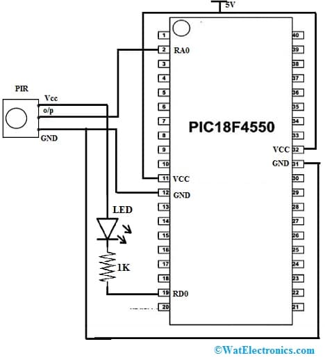
Interfacing the PIR sensor with the PIC18F4550 Microcontroller is shown below. In this interfacing, when motion is detected the LED will turn ON. The required components to make this interfacing mainly include; PIR Sensor, 5mm LED, PIC18f4550, PICKit 4 MPLAB, connecting wires, and breadboard.
PIR sensor or passive infrared sensor is used to detect IR heat radiation from living objects. This sensor has two slots which are connected to a differential amplifier. Once an immobile object is before the PIR sensor, then the sensor’s two slots will get a similar amount of radiation, so the output will be zero. Similarly, whenever a moving object is before the sensor, then the sensor’s slot will get more radiation as compared to another slot. So this makes the o/p low or swing high. So the change within the output voltage is the outcome of the motion detection.
The connections of this interfacing follow as;

Interfacing PIR Sensor with PIC18F4550 Microcontroller
- The VCC pin of the PIR sensor is connected to pins 11 & 32 pins of the PIC microcontroller.
- The Output pin of the PIR sensor is connected to pin2 (RA0) of the PIC microcontroller.
- The GND pin of the PIR sensor is connected to pins 12 & 31 of the PIC microcontroller.
- Connect pins 11 & 32 of the microcontroller to Pin19 (RD0) through LED & 1K resistor.
Code
The required code for this interfacing is shown below.
#include <pic18f4550.h>
#include “Configuration_Header_File.h”
#define Motion_detection PORTAbits.RA0 /* Read the data of PIR sensor on this pin */
#define PORT_Dir TRISAbits.RA0 /* define for setting direction */
#define LED LATD0 /* LED need to connect to the PORT pin */
#define LED_Dir TRISDbits.RD0 /* define for setting direction */
void MSdelay(unsigned int val);
void main(void)
{
ADCON1=0x0F; /* this will make all the pins as a digital I/O pins */
PORT_Dir = 1; /* set as input port */
LED_Dir = 0; /* set as output port */
LED = 0; /* Firstly turned OFF LED */
OSCCON = 0x72;
while(1)
{
while(Motion_detection)
LED = 1; /* if motion is detected LED will turn ON */
LED = 0; /* if motion is not detected LED will turn OFF */
}
}
void MSdelay(unsigned int val)
{
unsigned int i,j;
for(i=0;i<val;i++)
for(j=0;j<165;j++); /*This provides 1 ms of delay for 8MHz Frequency */
}
Working
Once the connections are made, upload the above code into the microcontroller. As shown in the above interfacing, the PIR sensor’s o/p pin is connected to the microcontroller’s PORTA.0 pin. So if the motion of an object is detected, the pin goes HIGH & LED will turn ON. Similarly, if the motion is not detected then the pin goes LOW and the LED will turn OFF.
Once the module is powered, it needs about 30 to 50 seconds to warm up to function accurately. We should not keep this sensor near the Wi-Fi antenna, NodeMCU/ESP32 otherwise it impacts the performance of the PIR sensor. WiFi signals produce electromagnetic radiation, so this can interfere with the sensor and cause false detection. So keep the sensor & Wi-Fi antenna always as far as possible.
Applications
The applications of the PIC18F4550 microcontroller include the following.
- These microcontrollers are used in development boards for learners.
- PIC18F4550 microcontroller is used in temperature control systems.
- These are used in measuring & manipulating of the analog signals.
- These microcontrollers play a major role in different embedded systems like vending machines, coffee machines, etc.
- These are used in motor control systems & peripheral interface systems.
- These are used by makers & engineers in different projects due to their easy applications & features.
- This microcontroller is ideal for connectivity & low-power applications.
Please refer to this link for the PIC18F4550 Microcontroller Datasheet.
Thus, this is an overview of the PIC18F4550 microcontroller, pin configuration, specifications, architecture, interfacing, and its applications. The PIC18F4550 microcontroller belongs to the pic18f family and is one of the most advanced PIC microcontrollers from the microchip technology. This is an 8-bit & 40-pin based microcontroller that has 32KB of Program Memory, 2048Bytes RAM, 256Bytes of EEPROM Memory & 12MIPS of CPU Speed. Here is a question for you, what is PIC18F2550?