A Register in digital electronics is a device, used for storing instruction, any type of data, or a storage address. It includes a set of flip-flops (FFs) which are connected within series for storing multiple data bits. The data which is stored in these registers can be transmitted using shift registers. A digital circuit that uses a cascade of flip-flops by connecting one flip-flop output to another flip-flop input is known as a shift register. a shift Register is a group of FFs used to store multiple data bits where these bits can be made to shift in the registers by applying CLK signals. The shift registers that will move the bits toward the left side are known as SLR (Shift left register) and the registers that move the bits toward the right side are called SRR (Shift right register). There are different types of shift register ICs used in digital electronics are; 74HC164, CD4014, 74HC595, etc. This article discusses an overview of the CD4014 shift register, its working & its applications.
What is the CD4014 Shift Register?
The CD4014 IC is an 8-stage shift register that belongs to the 4000 series family and is based on CMOS logic. This shift register includes serial or parallel input/ serial output. This IC is made with flip flops where the standard CLK signal provides transition signals for all the FFs, so they are synchronous with each other. The mode selection pin of this IC is available for controlling the input mode. In addition, control pins allow inputs to the shift register.
CD4014 Shift Register is designed with P-channel & N-channel enhancement mode transistors. This IC’s operating voltage ranges from 5 to 20 volts, which is significantly higher as compared to the contemporary logic family. This IC also has a buffered output that develops characteristics by simply providing extremely high gain. These IC inputs are protected against fixed discharge by diodes.
Working
This IC allows you to obtain several values at once as an input and after that shift them out by simply controlling four o/p pins in parallel. This IC has a serial or parallel control input pin that decides whether the data moves into the register in a serial or parallel manner.
Once the serial or parallel control input value is low, then data is shifted serially into the register. Similarly, when the control input value is high then the data is shifted parallel into each stage. This shift register has a common CLK that shifts data in a serial or parallel manner. The data at the positive edge of the CLK signal is moved into the shift registers in a serial/parallel manner based on the serial or parallel condition of the control input pin.
Pin Configuration:
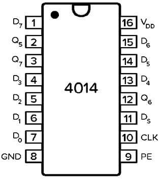
The pin configuration of the CD4014 shift register is shown below. This IC includes 16 pins and each pin and its functionality are discussed below.

CD4014 Shift Register Pin Configuration
- Pins (1, 4, 5, 6, 7, 13, 14 &15): These are parallel i/p data pins which are indicated as PI 1 to PI 7.
- Pins (2, 3 &12): These are output pins which are indicated as; Q6, Q7 & Q8.
- Pin8 (VSS): It is a GND pin or negative power supply.
- Pin9 (INPUT P/S): It is a parallel or serial control i/p pin.
- Pin10 (CLOCK): It is a CLK pulse or input signal.
- Pin11 (SERIAL IN): It is a serial input data pin.
- Pin16 (VDD): It is a positive (+ve) terminal of the voltage supply.
Features & Specifications:
The features and specifications of the CD4014 shift register include the following.
- It is a 16-pin shift register IC.
- This IC is available in PDIP, PDSO & GDIP packages.
- It is an 8-stage parallel i/p/serial o/p shift register.
- It has a completely static operation.
- Its operating voltage ranges from 3Volts to 18Volts.
- Its input current maximum is 1 µA @18 V
- It has high noise immunity – 0.45.
- Its operating temperature ranges from -55°C to +125°C.
- Its propagation delay is – 320nsec.
- It is compatible with low-power TTL.
- Its input lines are – 9.
- Its output lines are – 3.
Equivalents & Alternatives
The equivalent CD4014ICs are; MC14014, NTE4014, HEF4014/ HCF4014 and an alternative CD4014ICs are; 4021, 74HC165, 74HC166 & 74HC198.
CD4014 Shift Register Circuit
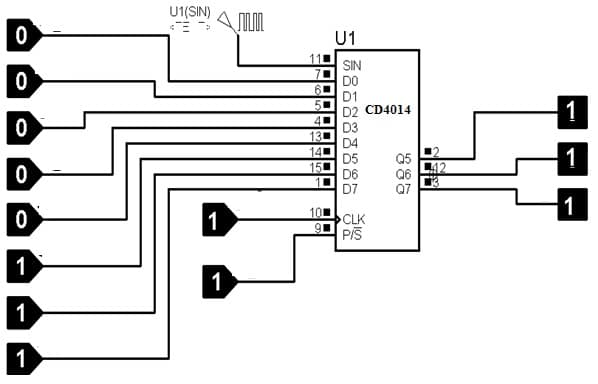
This IC is an 8-bit static shift register that includes 16 pins where seven pins from INPUT PI 1 to INPUT PI 7 are accountable for parallel data input. In addition, it has three o/p pins which range from Q6 to Q8. The parallel data transfer using the CD4014 shift register is shown below.
By using this circuit, the parallel data transfer can be done. Firstly, we must set the P/S pin to active high for selecting parallel data transfer. So, a CD4014 shift register IC will jam the available data on the pin11 like SIN. So it will shift the data only from parallel pins like D0 to D7.
To load data through the parallel inputs, need to set the Parallel Enable pin HIGH and provide input values to the D0 – D7 parallel input pins. The parallel data will be loaded into the shift register on the next increasing CLK edge on the CLK pin. For shifting the data single position, utilize the CLK pin while maintaining the Parallel Enable pin LOW. The clock pin moves the data on every rising edge.
At first, we provide input to parallel input pins like 00000111. When we give CLK cycles a positive edge to the IC, 111 will appear at the output pins because MSB bits comes first. Likewise, we provide 00000100 & 00000101 logic inputs. As a result on each positive CLK edge, respective logic will appear at the o/p pins.

CD4014 Shift Register Circuit
The advantages of parallel data transfer are; that several bits are transmitted at once and it is faster as compared to serial data transfer. This data transmission needs less complex electronic components as compared to serial.
Similarly, serial data transfer can be done by using this IC. So the data is transmitted bit-by-bit to the o/p. To choose a serial shifting mode in this IC, we need to set the P/S pin of IC to logic zero. Once the logic input like 00000001 is given at the i/p of serial pin then the output will start to show on Q6 to Q8 pins after the seven CLK cycle, because input signals at first are active low.
Applications
The applications for the CD4014 shift register include the following.
- CD4014 shift register is used for parallel to serial conversion of data.
- It is a general-purpose register used to perform data queuing.
- This IC is very useful in circuits that deal at a time with a large number of inputs.
- This IC is used for mainly the demultiplexing of data.
- These shift register ICs are used in pulse extenders and delay circuits.
- These are used in Digital memory circuitry like computers, data processing systems & calculators.
- These are used for data line de-multiplexing within communication lines.
Please check this article for How to Choose a Shift Register, 74LS74 D Flip Flop Datasheet.
Please refer to this link for the CD4014 Shift Register Datasheet.
Thus, this is an overview of the CD4014 shift register, pin configuration, features, circuit, working, and its applications.
The CD4014 is a CMOS IC that includes one serial input & eight parallel input pins for preloading the register. This IC can be used as a parallel-to-serial converter. This IC is made with D FFs which are connected in series so that every bit can be moved to the next FF on each clock pulse. Here is a question for you, what is the SIPO register?