An instrumentation amplifier or in-amp is a differential amplifier that includes a differential input & an output where these devices are used for amplifying the difference between two input voltage signals while refusing any signals that are very common to two inputs. These devices are used in test & measurement equipment of industrial, data acquisition, medical & measurement applications. There are different instrument amplifier ICs are there like INA33, AD623, INA128, LT1167, MAX4194 & AD8221. This article discusses an overview of the INA333 instrumentation amplifier, its working, and its applications.
What is INA333 Instrumentation Amplifier?
The INA333 IC is a high-precision & low-power instrumentation amplifier used in a wide range of portable applications because of its small size, flexible three-op-amp design & uses low power. This amplifier has rail to rail feature and it works at an extremely low current so that it can be used in battery-operated applications. This instrument amplifier has buffer amplifiers that are connected to their input pins so that it eliminates the requirement of impedance matching.
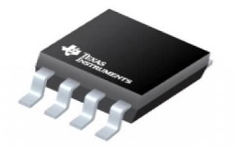
INA333 IC
The INA333 amplifier provides extremely low offset voltage, outstanding offset voltage drift & high CMRR. This amplifier operates with low power supplies like 1.8V & quiescent current is 50µA only so it is ideal for battery-operated systems. This amplifier also provides very low noise density that extends down to DC with auto-calibration methods to ensure outstanding precision above the extended industrial temperature range.
The INA333 instrumentation amplifiers are AEC-Q100 qualified which means that the device has approved the particular stress tests & guarantees a certain level of reliability or quality so that it can be used in automotive applications.
Pin Configuration:
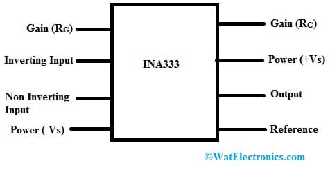
The pin configuration of the INA333 instrumentation amplifier is shown below. This amplifier IC includes eight pins which are discussed below.
INA333 PIn Configuration
Pin1 (Gain (Rg)): It is an inverting gain terminal used to connect to a resistor for setting gain value.
Pin2 (IN-/ Inverting Input): It is an Inverting i/p pin of the operational amplifier.
Pin3 (IN+/Non- Inverting Input): It is a non-inverting i/p pin of the operational amplifier.
Pin4 (-Vs/Power): It is a negative (-ve) supply terminal.
Pin5 (Reference): It is an o/p reference i/p and is connected normally to common.
Pin6 (Output): It is an o/p pin of an operational amplifier.
Pin 7 (+Vs/Power): It is a positive (+ve) supply terminal.
Pin8 (Gain (Rg)): It is a non-inverting gain terminal and is connected to a resistor for setting gain value.
Features & Specifications:
The features and specifications of the INA333 instrumentation amplifier include the following.
- It is a rail-to-rail instrumentation amplifier
- It includes one channel.
- It uses very less power.
- This amplifier provides excellent accuracy.
- These are available in small sizes.
- It is a versatile op-amp.
- It provides extremely low offset voltage.
- It is accessible in both 8-pin WSON & VSSOP surface-mount packages.
- Its operating voltage supply is 5.5 V.
- Its slew rate is 0.16 V/us.
- Its common mode rejection ratio or CMRR is 100 dB.
- Its input bias current (Ib) is 1.4nA.
- Its input offset voltage (Vos) is 10uV.
- Its operating current supply is 198uA.
- Its gain is 1000 V/V.
- Its bandwidth is 150 kHz.
- It is available in 8-Pin SOIC, VSSOP & PDIP packages.
- Its low offset voltage maximum is 25 µV.
- Its low drift is 0.1 µV/°C.
- Its low noise is 50 nV/vHz.
- It has a low i/p bias current maximum is 200 pA.
Equivalent & Alternatives
Equivalent INA333 instrumentation amplifier is AD623 and alternative instrumentation amplifiers are: AD620, LM4871, JRC4558 & IC6283.
Schematic Diagram of INA333 Instrumentation Amplifier
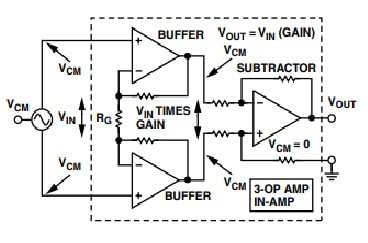
INA333 is a low-power instrumentation amplifier that provides excellent accuracy. It is a flexible three-op amp design which makes them used in a wide range of handy applications. In the following schematic diagram, an external single resistor simply sets from 1 – 1000 any gain.
Schematic Diagram of INA333 Instrumentation amplifier
Instrumentation amplifiers provide extremely low offset voltage, outstanding offset voltage drift & high CMRR. These amplifiers work with low power supplies like 1.8V & their quiescent current is 50µA only which makes them to use in battery-operated systems. The INA333 amplifier offers a very low noise density that expands downward to DC. The INA333 IC is available in both 8-pin WSON & VSSOP surface-mount packages. This amplifier’s specified temperature range is–40°C to +125°C. This module is used in many applications which include, ECG amplifiers, bridge amplifier pressure sensors, weigh scales, thermocouple amplifiers, medical instrumentation, and RTD sensor amplifier.
The instrumentation amplifier with three op-amps in the above circuit operates in the same conditions. Similar to the operational amplifier circuit, the instrumentation amplifier’s input buffer amplifiers pass the common-mode signal throughout at unity gain. On the contrary, the signal can be amplified through both buffers.
The output signals of two buffers connect to the subtractor part of the instrumentation amplifier. Here, the differential signal can be amplified whereas the common-mode voltage is attenuated. Comparing the two circuits, both give signal amplification although due to its subtractor section, this amplifier will reject the common-mode voltage.
INA333 Instrumentation Amplifier Circuit
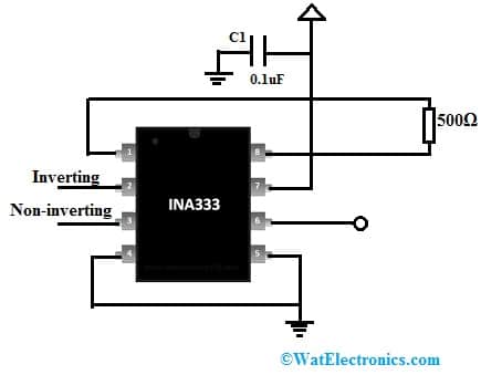
The INA333 instrumentation amplifier needs a resistor to simply set its gain value. A basic instrumentation amplifier circuit which is commonly used in different applications is shown below.
INA333 Instrumentation Amplifier Circuit
In the above circuit, the INA333IC is powered through pin 7 (+Vs/Power) whereas pin 4 (-Vs/Power is connected to the GND terminal. This circuit uses +5V single power supply. The pin 2 of this IC or non-inverting pin & the pin 3 or inverting pin are simply connected to the signal which has to be increased or contrasted based on the Op-Amp application.
The pin 5 of this IC like the Reference pin is usually grounded with pin 4 (-Vs/Power). Here the pin5 is used to direct the o/p towards a voltage whenever the difference voltage between the inverting & noninverting terminals is 0 Volts.
This amplifier’s Gain can be set by connecting the correct resistor value across pin 8 (+Rg) & pin 1 like –Rg. The value of the resistor used in this circuit is 500Ω to set the operational amplifier at a 100 gain value. To calculate the value of the gain of an op-amp, the following formula is used.
G = (49.4 kΏ / RG) + 1
INA333 is an Instrumentation Amplifier in ECG:
The INA333 is an instrumentation amplifier commonly used in electrocardiogram (ECG) applications. It plays a critical role in amplifying and conditioning the weak electrical signals generated by the heart to produce a clear and reliable ECG waveform. let’s see how INA333 is useful in an ECG device.
-
Signal Amplification: The ECG signal produced by the heart is relatively low in amplitude (typically in the millivolt range). The INA333 acts as an amplifier, increasing the signal magnitude to a more measurable level. It provides a high gain, typically around 100 to 1000, enabling the weak ECG signals to be easily detected and further processed.
-
Noise Rejection: The INA333 incorporates a high common-mode rejection ratio (CMRR) and differential input configuration. This allows the amplifier to reject common-mode noise signals that may be present, such as power line interference or electromagnetic interference (EMI). By canceling out these unwanted signals, the INA333 helps ensure a clean ECG waveform with minimal noise interference.
-
Filtering and Bandwidth Adjustment: The INA333 can be used in conjunction with external resistors and capacitors to implement additional filtering and adjust the bandwidth of the ECG signal. This helps eliminate high-frequency noise and unwanted artifacts, allowing for better signal fidelity and accurate representation of the cardiac activity.
-
Input Impedance: The INA333 offers a high input impedance, typically in the megaohm range. This high input impedance minimizes the loading effect on the ECG electrodes and ensures that the electrical signals from the body are not significantly attenuated or distorted due to the amplifier’s input impedance.
-
Single-Supply Operation: The INA333 can operate on a single power supply, typically in the range of 2.7V to 5.5V. This makes it suitable for portable or battery-powered ECG devices, as it enables low-power operation and simplifies the overall circuit design.
-
Low Power Consumption: The INA333 is designed for low power consumption, making it suitable for battery-operated ECG applications. Its low power consumption helps extend the battery life of portable ECG devices.
INA33 in ECG Circuit
ECG or Electrocardiography is the reading of the electrical activity of a person’s heart over a period of time. Electrocardiograms are ECG measurement devices that are used in the medical & investigation fields. The INA33 Instrumentation Amplifier in the ECG circuit is shown below.
The required components to make this circuit mainly include resistors like R1, R2, R4, R6, R7-1K, C2-47n, R4–1K, C1-1u, C2, C4-47n, C6 & C8-33p, C9-330P, C7-330P, C5-33P, RG1, RG2- 10K, INA333, OPA333-2, R5& R13- 1M, R3-10K, R14 & R16-1M. Connect the circuit as per the circuit diagram shown below.
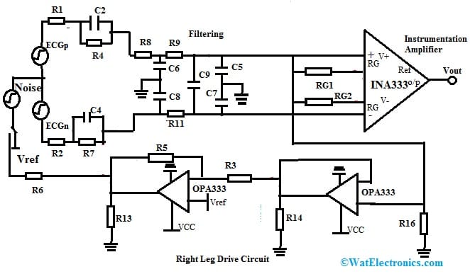
INA33 Instrumentation Amplifier in ECG
This circuit includes three stages amplifier, filtering, and right leg drive. The main function of an ECG is to amplify the measured small signal from the heart, to filter outside & inside noise. Here, the amplification can be implemented with a differential amplifier while filtering is done throughout common mode & differential mode filtering. The right leg drive circuit in this circuit helps in canceling noise & also maintains the common mode voltage.
Amplifier Stage
ECG signals have a small range that ranges from the microvolt to the millivolt so the measured signals need to be amplified to be understood better.
A typical biopotential amplifier has high input impedance, designed mainly for security first because the amplified signal is being drawn from an alive organism thus safety measures should be taken to avoid small shocks. Here, to limit the current flow throughout electrodes to secure levels, isolation & protection circuits are utilized.
The amplifier’s output impedance must be extremely low for driving any outside load by the least distortion. An instrumentation amplifier has two stages that make it meet ideal biopotential amplifier characteristics. So here, the primary stage is known as the input stage of the instrumentation amplifier followed by the gain stage. So this stage supplies ideally no common-mode gain, and common-mode noise can be eliminated. This instrumentation amplifier includes three operational amplifiers which provide high input impedance to the input stage & its configuration provides high CMRR & high gain.
The input stage of the instrumentation amplifier buffers the stage of gain. At last, the input stage outputs are the gain stage inputs which have less impedance & provide a differential gain. So this amplifier only amplifies the differential component by a gain to provide a high CMRR.
Filtering Stage
ECGs have noise internally & externally so these can be digitally filtered throughout analog practices. So analog BSF (band stop filter) is used for modulating 60 Hz noise from power lines depending on the values selected for the resistor, capacitor & inductor. These filters help in removing outside noise because of the frequency of a heartbeat.
Right Leg Drive
The right leg drive circuit in this circuit decreases the interference from the instrumentation amplifier. It is achievable to increase an ECG signal & also create a DC common mode bias off the inputs electrically for the differential amplifier. But, whenever this is done then there is huge susceptibility mainly for the common mode interference wherever the requirement for the right leg drive comes in. So this right leg drive reverses & strengthens back the standard common mode signal into the right leg of the patient. This act will cancel 60 Hz noise from AC power & creates a very clean output ECG signal. In the feedback loop, more gain is used to improve the CMRR. In this way, the noise will be canceled and relaxes the required attenuation from the CMRR of the amplifier.
INA33 Instrumentation Amplifier with RTD
RTD Sensor: The RTD sensor is a resistance temperature detector that changes its resistance with temperature variations. The RTD is connected in series with R1, forming a voltage divider.
Voltage Divider: R1 and the RTD sensor form a voltage divider. The resistance of the RTD changes with temperature, causing a change in the voltage across the RTD.
INA333 Instrumentation Amplifier: The voltage across the RTD is amplified by the INA333 instrumentation amplifier. The INA333 is connected in a differential configuration, with its inputs connected to the voltage divider.
Gain Setting Resistor (RG): The gain of the instrumentation amplifier is determined by the RG resistor. The value of RG sets the amplification factor, which can be adjusted to suit the required temperature measurement range.
Output (Vo): The amplified output voltage (Vo) of the INA333 is proportional to the temperature measured by the RTD sensor.
Power Supply: The INA333 instrumentation amplifier requires a dual power supply, typically within the range of ±2.25V to ±18V. The positive and negative power supplies (+VS and -VS) are connected to the appropriate pins of the INA333.
Ground (GND): Connect the ground terminal of the INA333 to the common ground of the circuit.
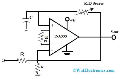
INA33 Instrumentation Amplifier with RTD
This circuit measures the temperature using the RTD sensor, amplifies the small changes in resistance with temperature using the INA333, and provides a corresponding output voltage proportional to the temperature. The amplified output (Vout) can then be further processed or converted to temperature values using appropriate calibration and conversion techniques. It can be connected to a microcontroller . Let see how it can be connected.
INA33 interface to Microcontroller:
The INA333 can be connected to a microcontroller to interface with and process the amplified analog voltage signals. The microcontroller can receive the amplified output from the INA333, convert it into a digital value using an analog-to-digital converter (ADC), and perform further signal processing, calibration, and data analysis.
Here’s how the INA333 can be connected to a microcontroller:
- Amplified Output to Microcontroller ADC Input: Connect the output of the INA333 (Vout) shown above to one of the analog input pins (ADC input) of the microcontroller. The amplified voltage signal represents the measured quantity (e.g., temperature in the case of an RTD sensor) and needs to be converted into a digital value for processing by the microcontroller.
- Reference Voltage Connection: If the INA333 is using a reference voltage (Vref) for operation, connect the reference voltage source to the REF pin of the INA333. Additionally, ensure that the microcontroller’s ADC reference voltage matches the reference voltage used by the INA333 to ensure accurate conversions.
- Power Supply Connection: Provide the required power supply voltage (Vcc) to the V+ and V- pins of the INA333. The voltage should be within the specified operating range of the INA333.
- Ground Connection: Connect the ground (GND) pin of the INA333 to the ground of the microcontroller to establish a common ground reference for proper signal measurements.
- Microcontroller Programming: In the microcontroller firmware, configure the ADC to read the voltage from the INA333’s output pin. The ADC will convert the analog voltage into a digital value, which can then be further processed and used for temperature measurement or other applications.
- Signal Processing and Calibration: In the microcontroller code, perform any required signal processing, calibration, and unit conversion based on the digital values obtained from the ADC. For RTD temperature measurements, you might apply appropriate calibration coefficients and perform linearization based on the RTD characteristics.
By connecting the INA333 to a microcontroller, you can easily integrate precise and accurate analog signal measurements into your microcontroller-based applications. This allows for flexible and efficient data acquisition, processing, and control based on the amplified signals from the INA333, making it suitable for a wide range of applications, including temperature sensing, pressure sensing, and other sensor-based measurements.
Applications
The applications of the INA333 instrumentation amplifier include the following.
- INA333 instrumentation amplifiers are used in ECG, Thermocouple, RTD sensor & bridge amplifiers.
- These amplifiers are used in portable and medical instrumentation.
- These instrumentation amplifiers are used in weighing scales, pressure sensors & data acquisition.
- These are used in a broad range of portable applications.
- It is used in battery-operated applications.
- This amplifier removes the need for impedance matching so that it can be used in test & measurement equipment.
- It is used to decrease the unwanted noise that is chosen by the circuit.
- These amplifiers are extremely helpful because of their high CMRR.
Please refer to this link for How to Choose an Instrumentation Amplifier.
Please refer to this link for INA333 Instrumentation Amplifier Datasheet.
Thus, this is an overview of the INA333 instrumentation amplifier, pin configuration, features, specifications, circuit, and applications. The INA333 instrumentation amplifier is ideal for different applications like sensor amplification, industrial process control, medical instruments, and audio amplification due to its low power consumption, excellent accuracy & high CMRR. The INA333 amplifier is a flexible & reliable option for various applications because of low i/p bias current, wide voltage supply range, low i/p offset voltage & drift, rail-to-rail o/p & low quiescent current. Here is a question for you, what is the function of an operational amplifier?