Flip flops are basic building blocks in sequential circuits which are used as data storage elements for storing a single bit of data. These storage elements include two states which are represented by a “one” & a “zero”. When these elements are used in an FSM (finite-state machine), then the output & next state of this not only depends on its present input but also depends on its present state. Generally, flip-flops maintain a particular state until & unless directed through the input to change that state. There are different types of flip flops available like SR, J-K, T & D Flip Flop. This article discusses a 74LS73 dual jk flip flop, specifications, working, and its applications.
What is 74LS73 Dual JK Flip Flop?
The 74LS73 is a dual JK flip-flop IC that includes two separate JK flip-flops by individual J-K, CLK & direct clear inputs. So each JK FF in this IC is used separately based on the application. The 74LS73 IC is a positive pulse-triggered FF. The J-K input of this IC can be loaded into the master whereas the CLK is high & transmitted to the slave above the high (H) to low (L) transition. The flip flops in this IC have a different structure and they both do not depend even on each other. So the user could even utilize a single FF without using the second FF. This JK FF IC is utilized in latching applications & they can work as a tiny programmable memory in different projects. The 74S73 dual jk flip flop IC is the best option when we require two JK flip flops simultaneously.
Pin Configuration:
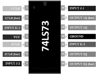
The pin configuration of the 74LS73 dual JK flips flop is shown below. This IC includes 14 pins where each pin & its function are discussed below.

74LS73 IC Pin Configuration
Pin 1 (1 CLK): This is the CLK pin of the first JK FF. Here, a change of pulse can be used for changing the state.
Pin 2 (1CLR (BAR)): This is the reset pin of the first JK flip-flop. Here, the LOW pulse is used to clear the flip-flop data.
Pin 3 (INPUT K-1): This is the i/p pin used for sending the bit toward the JK FF.
Pin 4 (VCC): This pin provides the power supply to the JK FF to the entire chip.
Pin 5 (2CLK): This pin is utilized to provide the CLK signal to the 2nd JK FF in IC. Here, pulse change from LOW (L) to HIGH (H) is used for changing the state.
Pin 6 (2CLR (bar)): This pin is used as a reset pin through the 2nd JK FF. Here, the LOW pulse is utilized to reset the data from the FF.
Pin 7 (INPUT J-2): This pin is used to send the 2nd i/p of JK FF.
Pin 8 (OUTPUT 2Q (bar)): This pin is used as an inverted o/p of the 2nd JK FF.
Pin 9 (OUTPUT 2Q): This pin is used as the non-inverted o/p of the 2nd JK FF.
Pin 10 (INPUT K-2): This pin is used as an i/p pin for the 2nd JK FF.
Pin 11(GROUND): This is a ground pin and is used to apply the GND of the power supply.
Pin 12 (OUTPUT 1Q): This pin provides s the non-inverted o/p from the primary JK FF.
Pin 13 (OUTPUT 1Q (bar)): This pin provides the inverted o/p from the primary JK FF.
Pin 14 (INPUT J-1): This pin is used as a 2nd i/p for the primary JK FF.
Features & Specifications
The features and specifications of the 74LS73 dual jk flip flop are discussed below.
- This IC includes two separate negative edge-triggered JK FFs.
- Clear i/p resets the o/p.
- The switching times of this IC are fast.
- Its operating temperature is 70°Centigrade.
- It has typical TTL switching voltages.
- This IC works for all types of TTL or EMOS devices.
- It stores a single bit although it has the capacity to provide the toggle & no change state.
- This IC stores two bits simultaneously.
- This FF IC doesn’t contain any invalid or error state.
- Its charge storage temperature ranges from -65 to 150 degrees.
- This IC is available in two packages PDIP & SOIC.
- It is manufactured by Texas Instruments.
- Its type of function is JK-master-slave.
- It has inverting/non-inverting polarity.
- Its input & output type is TTL
- Its propagation delay time is 20 ns.
- Its maximum output current is; – 0.4 mAmps.
- Its minimum output current is 8 mAmps.
- The number of i/p lines is 3.
- The number of o/p lines is 1.
- Its mounting style is through-hole.
- Its operating voltage supply ranges from 4.75V to 5.25V.
- Its equivalent 74LS73 dual jk flip flop is; MC74HC73A whereas alternative 74LS73 dual jk flip flops are; 74LS76, 4027B & 74LS107.
Working
First, the 74LS73 dual JK flip flop can be understood by the SR latch. The SR latch includes two inputs Reset & set. The output of this must be in a high state when a minimum of one pin & another pin must be low state. SR latch functions with four logic states. Whenever both the i/p pins are different but there are equal outputs. When both inputs are the same, then the o/p will become invalid. To overcome this issue, an internal CLK has been installed within this flip-flop for controlling the change within the output by the input condition.

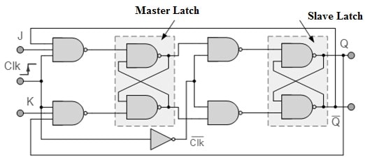
74LS73 Dual JK Flip Flop
JK flip flop in the above diagram includes two SR latches & four NAND logic gates. The primary SR latch is utilized as Master whereas other SR latch can be used as Slave. Here, the input toward Master SR Latch is provided by the Slave SR latch & two NAND logic gates. The Slave latch output to the Master latch helps the FF to toggle. The Master SR latch input signal is connected directly to the logic Gates. So the logic gates output has been given to the CLK pin. Here, the only CLK pin allows the NAND logic gate to provide the o/p to the SR master latch once the CLK gets an increasing pulse.
Once the clock pin is LOW then there is no output because it will be ignored in this case. The Master Latch o/p is given to the Slave latch once the pulse will be HIGH state to LOW to the i/p gate of the Slave Latch. So this clocking procedure between both the Master & Slave latches will make the FF transmit the data from the master latch to the slave latch through a timing signal. The truth table of the JK flip-flop is shown below.
|
CLK |
J | K | Q | Q’ |
State |
|
1 |
0 | 0 | Q | Q’ | No change within the state. |
|
1 |
0 | 1 | 0 | 1 | Q resets to zero. |
| 1 | 1 | 0 | 1 |
0 |
Q sets to one. |
| 1 | 1 | 1 | – | – |
Toggles |
74LS73 Dual JK Flip Flop Circuit
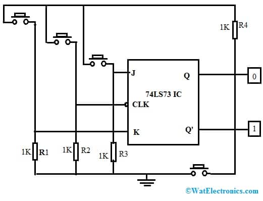
74LS73 IC includes two JK flip-flops triggered with a negative edge. This IC works with +5Volts and a typical connection diagram of the JK flip-flop is shown below.

74LS73 Dual JK Flip Flop Circuit
In the above JK flip flop circuit, the input pins are J & K pins whereas the output pins are Q & Q’. In the above circuit, both the i/p pins are pulled to the ground side with a 1k resistor so that we can keep away from the pin within the floating condition. Whenever the button in the circuit is pushed then the pin will be connected to the voltage supply and when the button is not pushed then the pin will be connected to GND.
The reset button must be pushed up with a 1K resistor & when grounded it will return the FF. Here for the FF, the CLK signal is responsible to change the output condition. The output of the FF will be changed simply throughout the increasing edge of the CLK signal. Here the CLK signal is just a push button however can be a kind of signal as a PWM. The FFs output condition can be decided from the above truth table.
In the IC normal operation, the reset pin is set to high & the known frequency CLK signal will be supplied toward the CLK pin, after that the J & K value will be changed depending on the i/p signals as well as the particular o/p will be attained on the Q & Q’ pins.
Where to use 74LS73 Dual JK Flip Flop/Applications
74LS73 dual jk flip flops are used in different applications like the following.
- Digital Electronics.
- Shift Registers.
- Latching Devices.
- Network Equipment.
- Memory or Control Registers.
- Personal Computers and Notebooks.
- Latching Devices.
- EEPROM Circuits.
- This FF is used in RAM.
- It controls the particular LED Pattern.
Please refer to this link for the 74LS73 Dual JK Flip Flop Datasheet.
Thus, this is an overview of 74LS73 Dual JK Flip Flop, pin configuration, features, specifications, circuit, and its applications. The JK flip-flop is the most frequently utilized flip-flop design, so it is considered the universal FF. Here is a question for you, what is a latch?