The MOSFET is an advanced type of FET, used to amplify or switch voltages within circuits. This is a voltage-controlled device and it overcomes the drawbacks of FETs like slow operation, moderate input impedance & maximum drain resistance. Whenever a voltage supply is applied to the gate pin of this transistor, then it will start conducting throughout the Source & Drain pins. MOSFET is classified into two types P-channel MOSFET & .N-channel MOSFET. There are many transistors available that fall under p- channel and n-channel categories. Among them, BS138 MOSFET falls under the N-channel MOSFET category. This article discusses an overview of BSS138 MOSFET, pin configuration, specifications, application circuit, and its applications.
What is BSS138 MOSFET?
The BSS138 MOSFET is an N−Channel enhancement mode MOSFET produced with Onsemi’s proprietary, DMOS technology & high cell density. These MOSFETs are available in the SOT-23 package and these are mainly designed to reduce on−state resistance and also supply strong, consistent, and quick switching performance. So these MOSFETs are perfect for high efficiency-based power management applications.
This BSS138 MOSFET has robust & compact nature, so it is suitable for portable applications like cell phones & power management circuits. This MOSFET is expensive as compared to its substitute 2n7002.
Pin Configuration:
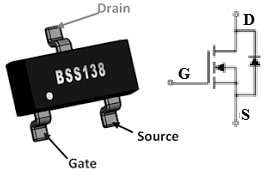
The pin configuration of BSS138 MOSFET is shown below. This MOSFET includes three pins which are discussed below.

BSS138 MOSFET Pin Diagram
- Pin1 (Source): This terminal allows the Electrons to enter the channel.
- Pin2 (Gate): This terminal controls the MOSFET biasing.
- Pin3 (Drain): Electrons leave through this terminal from the channel.
Features & Specifications:
The features and specifications of BSS138 MOSFET include the following.
- It is an N-Channel Logic Level MOSFET.
- Its Turn ON & OFF time is 20ns.
- Its continuous Drain Current or ID is 200mA.
- It comes in low on-state resistance.
- Its Gate threshold voltage or VGS-th is 0.5V.
- Its On-state resistance is 3.5ohms
- Its Drain to Source Voltage or VDS is 50Volts
- Its Gate threshold voltage or VGS-th is 1.5V.
- Its Gate source voltage is ±20V
- Its Max power dissipation is 360mW
- Its operating junction temperature ranges from -55°C – 150°C.
Alternative & Equivalent BSS138 MOSFETs
Alternative BSS138 MOSFETs are 2N7002, NTR4003, FDC666, 2N7000, FDC558, BS170,etc. Equivalent BSS138 P-Channel MOSFETs are; FDN358P & BSS84 and Its other N-Channel BSS138 MOSFETs are; IRF3205, BS170N, 2N7000, IRF540N, IRF1010E, etc.
Logic Level Converter Circuit using BSS138 MOSFET
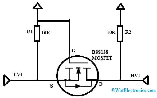
A logic level converter circuit is one type of special circuit, used to change the voltage from 5 volts to 3.3 volts and vice versa. The logic level converter circuit using bss138 MOSFET is shown below. This circuit can be built with BSS138 N-channel MOSFET, two 10k ohm resistors, a diode, and a 3.3Volts and 5Volts battery. Connect the circuit as per the circuit shown below.

Logic Level Converter Circuit using BSS138 MOSFET
Working
The logic level converter passes from high to low or low to high. In the above circuit, two pull-up resistors are used for understanding bi-directional level shifting. The input voltage is connected to every MOSFET terminal as shown in the circuit. The MOSFET used in this circuit is the N-channel enhancement type. The gate terminal of this transistor is connected to the 3.3Volts & the source terminal is connected to the low voltage (LV1) input pin. The drain terminal is connected directly to a high voltage i/p pin through a 10k ohm Pull up resistor by pulling this pin to logic 5 volts.
The diode in between the source & drain terminals is a PN junction that works like a barrier. So this permits to connection devices securely in every output without any problem. The LV1 & HV1 pins in the above circuit work as both i/p & p/p pins. So if you have to change the voltage from 3.3 volts to 5 volts, then you have to provide 3.3 volts to the LV1 pin and it provides 5 Volts output through the HV1 pin. Once there is no input given to the LV1 pin then the output at the HV1 pin will be 0v.
Advantages & Disadvantages
The advantages and disadvantages of BSS138 MOSFET include the following.
- The BSS138 MOSFET uses the most recent techniques to attain low on-resistance & high cell density.
- This MOSFET is very efficient & reliable.
- It is a low resistance & low i/p capacitance logic-level N-channel type MOSFET.
- It has a low gate threshold voltage.
- Its switching speed is very fast.
The disadvantages and disadvantages of BSS138 MOSFET include the following.
- It is expensive as compared to 2n7002 because it is an alternative.
- The BSS138 MOSFET is only applicable in low voltage & low current switching applications.
- The main drawback of this MOSFET is its low drain current; so it provides 200mA of continuous current & up to 1A of peak currents at the highest threshold voltage. So anything above that will harm the MOSFET.
Applications
The applications of BSS138 MOSFET include the following.
- BSS138 MOSFETs are mainly suitable for low current, low voltage-based applications which include gate drivers of power MOSFETs, controlling of small servo motors & other switching-based applications.
- This MOSFET is used as a switching device within ECUs or electronic control units.
- It is used in low-voltage and low-current applications.
- It is applicable in automotive electronics.
- It can be used in modern electric vehicles as power converters.
- It is used in DC to DC converts, logic level shifters, and e-Mobility applications
- These MOSFETs are used where low on-state resistance is necessary.
- It is used in power management-based applications.
- It is used in high-efficiency SMPS.
Please refer to this link for BSS138 MOSFET Datasheet.
Thus, this is an overview of BSS138 MOSFET, pinout, specifications, circuit working, advantages, disadvantages, and applications. The BSS138 is available in the SOT-23 package and the low threshold voltage & high switching speed of this MOSFET will make it an ideal choice for level shifter circuit-based applications. The N-channel MOSFETs are preferred in most of the applications as compared to P-channel MOSFETs because the movement of electrons is better than the movement of holes. These MOSFETs stay cool while working with high loads whereas P-channel type MOSFETs will turn hot. Here is a question for you, what is 2n7002 MOSFET?