MOSFET is the most frequently used 3-terminal device used to design integrated circuits so it brings a revolution in electronic circuits. MOSFETs are available in quite small and their manufacturing process is extremely simple. The analog and digital integrated circuits implementation is successfully done due to the MOSFET characteristics. So MOSFET circuits are analyzed in two ways like the small signal model & large signal model. The small signal model is derived depending on the parameter of the large signal model whereas the large signal model is nonlinear. This article discusses MOSFET circuits used in different applications.
MOSFET Circuits
The different electronic circuits using MOSFET are explained below which are used in different electronic projects.
MOSFET Motor Driver
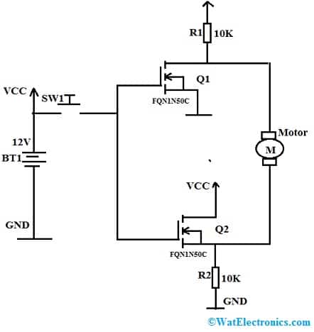
The motor driver circuit using N channel MOSFET is shown below. This circuit can be built with different components like 12V DC Battery or Adapter, switch, 10K Ohm resistors -2, FQN1N50C N Channel MOSFETs-2 & 12V DC Motor. Connect the circuit as per the circuit shown below.
MOSFET Motor Driver
In this motor driver circuit, the DC motor runs continuously in a single direction until once the switch is pressed, it reverses its direction and would be controlled by the other MOSFET. So this simple circuit is used as a Motor driver within different electronic projects. This motor driver circuit can be used with any Development board or Microcontroller to control the motor. This circuit is very simple to use and also has more control over the motor movements.
Working
In the above circuit, the Sw1 switch is connected directly to both the MOSFET gate terminals. MOSFETs source pins are connected to GND. Once both source terminals of MOSFET are connected to GND we will get the output for our DC motor in the drain pin of Q1 & source pin of Q2. The drain pin of Q1 is connected to vcc.
By connecting a switch between the battery & gate terminals of MOSFET, we can control the MOSFET by turning it ON/OFF. Once the switch is not pressed then MOSFET will be in open condition & the DC Motor in the circuit will get 12V from the drain terminal of the Q1 on its positive (+ve) pin and 0V from the Q2 transistor to the negative pin of the motor. However, when we push the button, the transistors will be in a saturation state. As a result, the motor gets 0V from the Q1 transistor & 12V from the Q2 transistor, so the motor’s rotation direction will be changed.
MOSFET Audio Amplifier
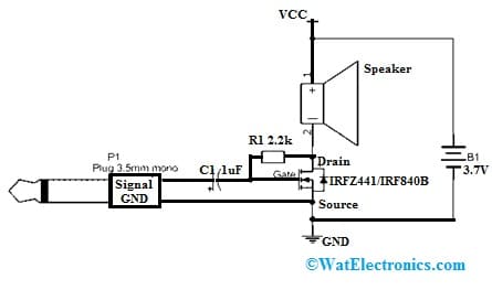
The MOSFET audio amplifier circuit is shown below. This audio amplifier circuit is very simple to design and is used to listen to the audio sound from any cell phone or laptop. This circuit can be built with an IRFZ44N MOSFET, plug 3.5mm mono, 1uF capacitor, resistor-2.2k, speaker, and 3.7V battery.
MOSFET Audio Amplifier
Connect the circuit as per the circuit diagram shown below. In this circuit, the IRFZ44N MOSFET drain pin is connected to the negative terminal of the speaker, the source pin is connected to the negative terminal of the battery or GND and the gate terminal is to the signal pin of 3.5mm mono. The resistor is connected between the base and drain terminals of MOSFET. The speaker’s positive terminal is connected to the positive terminal of the battery.
Working
This MOSFET audio amplifier circuit working is very simple like a basic transistor. Audio signals with less frequency come from audible devices but this signal is too low to listen through a Speaker. Here IRFZ44N MOSFET is used so it provides only the mono output. If you require Stereo output, you must use two IRFZ44N MOSFETs.
When the signal wire goes into the Gate terminal of the MOSFET then the MOSFET will Switches ON & OFF for the consequent frequencies. For this, the drain and source voltage of the transistor will vary. So the small signals will be amplified & bandwidth can also be high. Now we can hear the loud sound through the speaker.
MOSFET Timer
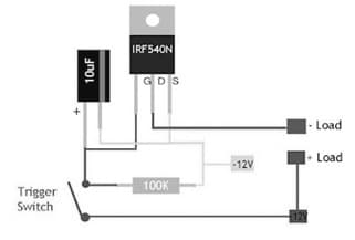
The MOSFET timer circuit is shown below. This circuit can be built with different components like 12V DC, 12V Lamp/ LED, 100K Ohm resistor, 10uF capacitor, switch, IRF540N MOSFET, etc. Connect the MOSFET timer circuit as per the circuit shown below.
MOSFET Timer
Working
The above MOSFET timer circuit uses the charging & discharging process of capacitors properties. Once we press the switch, the circuit runs so that the + 12V source voltage is directly connected to the gate terminal of MOSFET, then it will charge the capacitor immediately.
The output on the drain terminal, if we connect the lights, then the load-like light will turn ON instantly. Once the switch is released the light will not die instantly because the voltage current is still stored in the capacitor. As a result, the gate terminal of the MOSFET gets the voltage & the MOSFET will still turn ON. The on-state length is determined by the resistance of the resistor & capacity of the capacitor.
MOSFET Current Source
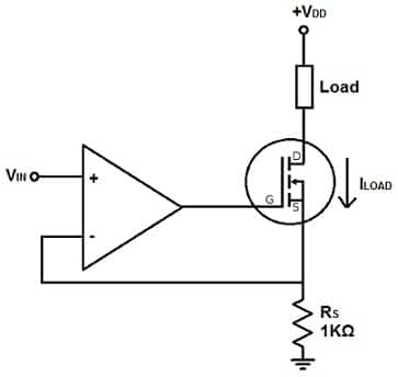
The mosfet current source circuit is shown below. This is a reliable current source circuit with below 1% error. This circuit provides stable output, and stable current without changing much. This circuit uses a MOSFET & op amp to make our current source. This circuit is very reliable as compared to a bipolar transistor-driven source. So, the leakage current amount is very small.
MOSFET Current Source
The required components to make this MOSFET current source mainly include LND150 N-Channel Depletion-type MOSFET, LM741 Op-Amp, 1KΩ resistor, and LED. Connect the circuit as per the circuit shown below.
Working
First, To power the op-amp, positive voltage need to apply to pin 7 like V+, and ground pin 4 like V-. So that it establishes power to the IC. This IC uses about a +5V supply. For this circuit, we need 2 other sources of power.
In this circuit, we need to provide power to the source of the transistor so that it gets power on a load. The load used in this circuit is LED. To the anode terminal of the LED, we connect the +ve voltage and the negative terminal of the LED is to the drain terminal of MOSFET. So it allows enough power to the LED .
The second input voltage required is for the noninverting terminal of the IC like 5V. The op amp’s inverting input samples the voltage across the ‘RS’ resistor after that it compares the applied voltage to the non-inverting input.
Generally, this IC is connected in such a way that it functions like a voltage follower. A voltage follower is a simple circuit where the output voltage is similar to the input voltage. Once the non-inverting terminal of the op-amp gets an input voltage & the inverting terminal is simply connected to the o/p of the op-amp, so this is the voltage follower setup.
Once the circuit is connected like a voltage follower, the output voltage will resist changes unless the i/p voltage changes. Thus, if the i/p voltage is stable at a particular value, then the output voltage will maintain a similar voltage as the input.
So, if the load current flowing throughout the source & drain of the MOSFET changes, then the output voltage through the op-amp changes in current, so that the output voltage will be stable, which stops bringing the current supply of load back to its baseline value.
Since the op-amp output is connected to the gate terminal of the MOSFET, the voltage at the gate terminal of the MOSFET varies if there are changes within the load current. If the load current is increased, then the op-amp provides a higher voltage output. This sequentially reduces the current supply so that it goes reverse to its baseline value. If there is a reduction within load current, then op-amp gives a lower voltage. So it increases the current so that it goes reverse to its baseline value.
So whatever voltage you feed into the op-amp’s non-inverting terminal above the RS resistor decides the load current like ILOAD. Since the ‘Rs’ resistor is a fixed resistor, then its value does not change so, ILOAD is stable. If there are any changes in the current, then this circuit compensates by raising or reducing the voltage at the gate terminal of the MOSFET. So this will enhance or reduce the current back toward its baseline value.
If we are utilizing Vin = 5V for the noninverting terminal of op-amp & a 1KΩ resistor, then this provides us 5mA of current. If you use an ammeter by placing it in series on either source or the drain side of the MOSFET, then must observe that it doesn’t differ much from its 5mA of the baseline value. If you desire to make the current source modifiable, then you have two options. Being the load current is determined by the resistance or voltage, you have to use a potentiometer to the voltage source so that you can change the current output.
MOSFET Voltage-Controlled Oscillator
Voltage controlled oscillator is a type of oscillator that generates output signal frequency above a large range based on the input DC voltage provided to it. These circuits are designed through different voltage control electronic components like Op-amps, transistors, varactor diodes, etc.
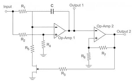
The MOSFEt voltage-controlled oscillator circuit is shown below. The required components to make this circuit are two op-amps, MOSFET, resistors, capacitors, etc. Connect the circuit as per the circuit shown below. The output of this circuit is a square wave whose frequency can be controlled through the input voltage.
MOSFET Voltage-Controlled Oscillator
Working
This circuit uses two op-amps where the first op-amp works like an integrator whereas the second op-amp works like a Schmitt trigger. In this circuit, the voltage divider arrangement is implemented so that half of the control voltage is provided as input to the +ve terminal of the first op-amp. At the negative terminal, the same voltage range is maintained. This is to maintain the voltage drop across the R1 resistor like half of the control voltage.
Once the MOSFET in the above circuit is in ON condition, the flow of current from the resistor ‘R1’ will supply throughout the MOSFET. So the R2 resistor has a similar voltage drop, half the resistance & twice the current like R1. So, the additional current will charge the capacitor connected to the circuit. The first Op-amp should provide a slowly increasing o/p voltage to supply this current.
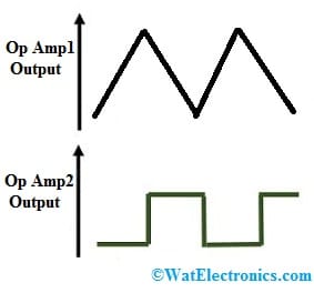
When the MOSFET in the circuit is in off condition, then the flow of current from the resistor ‘R1’ will discharge the capacitor. So, the output voltage obtained from the first op-amp will be decreased. Thus, a triangular waveform is produced as the output of the first op-amp.
Here, the second op-amp works as a Schmitt trigger. Here, the output of the first op-amp like a triangular wave is given as an input to this second op-amp. If the i/p voltage is high as compared to the threshold level, then the output of the second op-amp (op-amp2) will be VCC. If the i/p voltage is below as compared to the threshold level, then the output of the second op-amp will be zero. So, the output of the op-amp2 will be a square wave. These circuits are used in tone generators, function generators, PLL (Phase Locked Loop), FM (frequency modulation), and FSK (frequency shift keying).
The output waveforms of the MOSFET voltage-controlled oscillator are shown below. From the following waveforms, we can observe that, during the charging of capacitance, when the voltage increases at C1 then the Schmitt trigger output will be low. Similarly, now the voltage at the capacitor discharges then, the Schmitt trigger output will be high.
VCO Output Waveforms
Dont Miss:
- Enhancement MOSFET.
- P- Channel MOSFET.
- Difference Between BJT and MOSFET.
- Please refer to this for How to Select a Transistor.
Thus, this is all about an overview of MOSFET circuits which are very useful in making different electronics projects. The above circuits can also be realised using a BJT but there is a difference between a BJT and MOSFET control. To know what it is click here.