IRF3205 MOSFET is an N-Channel Power MOSFET based on Advanced Process Technology. This MOSFET was introduced by “International Rectifier” to generate very low on-resistance per silicon region. This MOSFET is different as compared to the normal MOSFET, where earlier MOSFETs come with a thick oxide gate layer & experience high input voltage whereas the current MOSFETs come with a thin-gate oxide layer without the capability to resist high voltage which means applying high voltage will affect the overall device performance drastically. These are suitable for power tools, high-power DC motors & industrial applications. This article discusses an overview of IRF3205 MOSFET – working with applications.
What is IRF3205 MOSFET?
The IRF3205 MOSFET is a high-current N-Channel MOSFET that can switch current upto 110A & 55V. This MOSFET has extremely low-on resistance like 8.0mΩ so it can be used in different switching circuits like DC-DC converters, motor speed control, Inverters, etc. This is very cheap and the most frequently available MOSFET. This MOSFET is suitable for switching circuits that operate < 55V & < 110A & the threshold voltage of this transistor is high, so it is not perfect for ON/OFF control through embedded controllers.

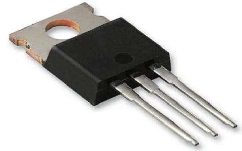
IRF3205 MOSFET
The IRF3205 MOSFET is simply made with the TO-220AB device package and the package is made with a combination of plastic & epoxy materials & the external cover is made with metal which is used as the medium for transferring heat. At the outer metal covering, a heat sink can be connected easily. This kind of packaging is mainly used for power-switching devices & driver circuit devices.
In this MOSFET, the current flow mainly depends on the movement of electrons & the current flow direction in this transistor is from drain (D) to the source (S) terminal. At the output terminal, the observed current depends on the applied voltage as input to the gate (G) terminal.
Working
The three terminals of this IRF3205 MOSFET are source, drain, and gate which are similar to the emitter, base & collector terminals of BJT. In this MOSFET, both the source & drain terminals are simply manufactured with n-type material whereas the MOSFET body with the substrate is manufactured by using p-type material.
To design this MOSFET, an extra silicon oxide layer is there on the substrate layer. The conduction process can be carried out through the movement of electrons to make this transistor as unipolar. An insulating layer is placed to separate the gate (G) terminal from the whole body of the MOSFET. So, the region between the source (S) & drain (D) is known as N-channel.
This channel is simply controlled through the present voltage level at the gate (G) terminal. If positive (+) voltage is applied to the MOS structure, then the distribution of charge within a device is altered in such a way that the charge carriers like holes available under the oxide layer must deal with a force so holes move in a downward direction.
But the bounded negative (-Ve) charges are connected permanently to the acceptor atoms & they are in charge to flock the depletion area. If more electrons are applied then they will enhance the overall channel conductivity thus causing change within the substrate to change to the N-type material.
Features & Specifications:
The features and specifications of IRF3205 MOSFET include the following.
- This is N-Channel power MOSFET.
- The process technology used in this is advanced.
- Very low on-resistance – 8.0mΩ.
- Dynamic dv/dt rating.
- Switching is very fast.
- Completely avalanche-rated.
- Continuous Drain Current or ID – 110A when VGS = 10V.
- Min Gate threshold voltage is 2V.
- The breakdown Voltage from Drain to Source is 55V.
- The gate-to-source voltage is ±20V.
- Rise time -101ns.
- The available package is To-220.
- Mounting is THT.
- The Ptot maximum is 150.0 W.
- The package is To-220.
- The pulsed drain current or IDM is 390A.
- Power dissipation or PD – 200W.
- On-state resistance from Drain to the source is (RDS (ON) – 8mΩ.
- Gate (G) to body leakage current (IGSS) is 100nA.
- Complete gate charge or Qg – 146nC.
- Reverse recovery time or trr is 69 – 104ns.
- Rise time or tr – 101ns.
- Peak diode recovery or dv/dt – 5V/ns.
- Junction temperature TJ ranges from -55 to 175℃.
- Thermal resistance from junction to the case or Rth j-c is 75℃/W.
IRF3205 MOSFET Pin Configuration:
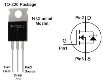
The pin configuration of IRF3205 MOSFET with a symbol is shown below. This MOSFET includes three pins which are discussed below.

IRF3205 MOSFET Pin Configuration
- Pin1 (Gate): This pin activates the MOSFET device.
- Pin2 (Drain): The current flows throughout this terminal.
- Pin3 (Source): The current flows out from this terminal.
Equivalent & Alternative MOSFETs
The equivalent IRF3205 MOSFETs are; IRFB3256, IRFB3307, IRFB3306, IRFB3006, IRF1405 and IRFB3206. The electrical specifications of these MOSFETs have almost the same, thus we can utilize these MOSFETs as the equivalent.
The alternative IRF3205 MOSFETs are; IRFZ44N, IRF1407, IRF1405, IRF3305, IRFB4110, IRFB3077. Other N-channel MOSFETs are; 2N7000, IRF540N, and FDV301N.
How to use IRF3205 MOSFET/Circuit Diagram:
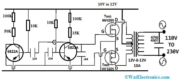
The inverter circuit using simple transistors is shown below. The required components to make this circuit are 6822A BJTs -2, IRF3205 MOSFETs -4 Resistors 100KΩ-2, 10KΩ -2,, 15KΩ-2, Non Polarized Capacitor 104 -3, 474J, 400V -1 and 12V – 0V – 12V, 10A center tapped transformer. Connect the circuit as per the below-shown diagram.

IRF3205 MOSFETs based Inverter Circuit
This is a simple DC-to-AC power inverter circuit using transistors. This circuit gives 100W -1000W output with 10V- 12V battery as well as 12V-0V-12V, 10A center tapped transformer.
The two NPN BJTs (bipolar junction transistors) are connected as an astable multivibrator (or) an oscillator where each transistor is half cycle out of phase at 50Hz to 60Hz frequencies. The four IRF3205 power MOSFETs simply amplify every half of the AC voltage produced by the oscillator. After that, this is fed to the center-tapped transformer. This transformer increases the voltage from 12V – 230V. But, one can enhance the output power by simply using additional power MOSFETs in parallel, high power transformer & high capacity power bank.
How to Connect IRF3205 MOSFET to a Microcontroller/Arduino Uno?
To connect an IRF3205 MOSFET to a microcontroller, the gate terminal of the MOSFET should be connected to one of the digital outputs of the microcontrollers.
- First, Connect the source terminal of the MOSFET to the ground of your circuit.
- Next, Connect the drain terminal of the MOSFET to the load that you want to control, such as an LED, motor, or relay.
- Connect a resistor between the gate terminal of the MOSFET. by setting the digital output pin to high or low. When the digital output pin is set to high, the MOSFET turns on and allows current to flow through the load. When the digital output pin is set to low, the MOSFET turns off and stops the current flow.
It is important to note that the voltage level of the microcontroller output pin should match the gate threshold voltage of the IRF3205 MOSFET. The gate threshold voltage of the IRF3205 is typically between 2 and 4 volts, so make sure that the output pin of the microcontroller can provide sufficient voltage to turn on the MOSFET. Additionally, a flyback diode should be connected in parallel with the load to protect the MOSFET from voltage spikes generated by the inductive load.
Applications
The applications of IRF3205 MOSFET include the following.
- IRF3205 MOSFET is used where high-speed load switching is required like Battery Backup systems, UPS, etc.
- It is used in various power supply applications.
- This MOSFET is used for controlling high current loads through embedded systems.
- Choppers.
- Power supply devices.
- High-speed switching devices.
- Speed controller circuit.
- Solar inverter.
- Motor drivers.
- Booster converter.
- Battery charger circuits.
- BMS or Battery management system.
- Inverter.
- Relay driver.
- It helps in making high-power-based audio amplifier circuits.
- Used in industrial & commercial applications.
- Fast Switching Applications.
- Solar Inverters.
1). What is the maximum voltage rating of the IRF3205 MOSFET?
A). The maximum voltage rating of IRF3205 MOSFET is 55V.
2). What is the maximum current rating of the IRF3205 MOSFET?
A). The maximum current rating of IRF3205 MOSFET is 110mA.
3). What is the gate threshold voltage of the IRF3205 MOSFET?
A). The gate threshold voltage (VGS) of the IRF3205 MOSFET is 10V.
4). What is the maximum power dissipation of the IRF3205 MOSFET?
A). The maximum power dissipation is 200 W at 25°C.
5). Can the IRF3205 MOSFET be used for high-frequency switching applications?
A). IRF3205 MOSFET is used where high-speed load switching is required like in Battery Backup systems, UPS, etc. They can also be used in power supply applications and for controlling high current loads through embedded systems.
6). Can the IRF3205 MOSFET be used in audio amplifiers?
A). This MOSFET is an ideal transistor to utilize in high-power audio amplifiers.
7). What is the package type of the IRF3205 MOSFET?
A). The package type of this MOSFET is TO-220AB.
8). What is the temperature range for the IRF3205 MOSFET?
A). The temperature ranges from -55°C to 175°C.
Please refer to this for How to Select a Transistor.
Please refer to this link for IRF3205 MOSFET Datasheet.
Thus, this is all about an overview of IRF3205 MOSFET – pin configuration, specifications, circuit, and applications. Here is a question for you, what is the function of a MOSFET?